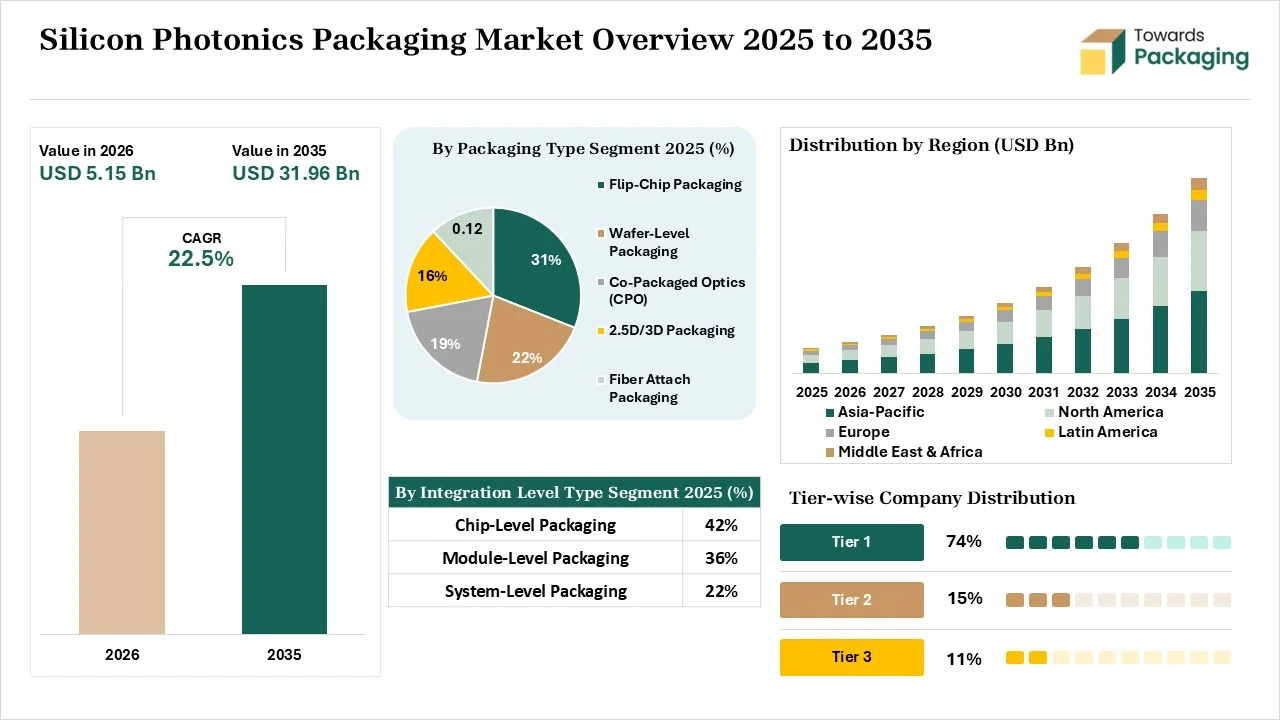
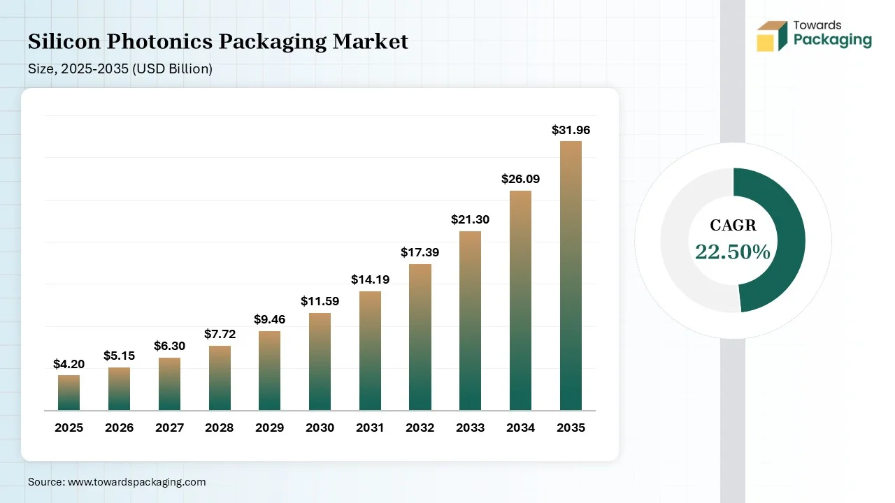
The Silicon Photonics Packaging Market is projected to grow from USD 5.15 billion in 2026 to USD 31.96 billion by 2035, registering a CAGR of 22.50% during the forecast period. The report covers detailed market size and revenue forecasts, segment-wise analysis, regional performance, competitive landscape, company profiles, value chain assessment, trade analysis, manufacturer and supplier insights, emerging opportunities, and key growth drivers shaping the industry.

Silicone photonics (SiPh) packaging is a type of integrated-optics technology that connects electronic chips and optical fibers. Its pillars are optical coupling, electrical integration, thermal management, and environmental protection. The challenges, such as high manufacturing cost, sub-micron alignment, and thermal management, occur in photonics packaging. The innovative silicon photonics packaging solutions are advanced assembly ecosystems, co-packaged optics, and monolithic integration. It offers benefits like extreme energy efficiency, CMOS compatibility, massive bandwidth, signal integrity, and reduced space. The primary applications of silicon photonics packaging are autonomous vehicle sensors, data centers, telecom, and optical quantum computing.
The silicon photonics packaging market growth is driven by the transition to co-packaged optics, increasing use of advanced transceivers, growing 5G rollouts, interest in miniaturized packaging, expanding quantum computing applications, growing AI infrastructure, explosion of data traffic, rise in heterogeneous integration, and innovations in automotive LiDAR.
The technological developments like EDA tools, computational modeling, machine vision, advanced software workflows, precision assembly, and advanced 3D integration are happening in the market. These technological developments are driven by data center congestion, high-density connections, and boosting energy efficiency. The major paradigm is the adoption of AI, which helps in tackling complex manufacturing issues.
AI helps in achieving energy-efficient connections and offers manufacturing precision. AI spots micro-variations and speeds up design cycles. AI enables co-packaged optics and easily solves the advanced bottlenecks that occur during packaging manufacturing. AI lowers insertion loss and increases the manufacturing yields. Overall, AI offers faster data transfer and easily solves manufacturing challenges.
Raw materials like glass, optical polymers, copper, gold, thermal interface materials, silicon-on-insulators, plastics, ceramics, index-matching adhesives, solder alloys, and metals are required.
Material processing involves deposition, etching, and substrate modification. Conversion includes mode-size conversion, polymer curing, and electro-optical conversion interfaces.
Package design focuses on electrical interconnects, mechanical enclosure, optical coupling, and thermal management. Prototyping involves mechanical package design, ADK utilization, die preparation, active or passive alignment, and multi-project packaging.
The flip-chip packaging segment dominated the market with 31% share in 2025 due to its high-speed performance. The focus on lowering signal delays and the burgeoning ML workloads increases the adoption of flip-chip packaging. The need for higher-speed data transmission and the rise in package profile miniaturization increase the use of flip-chip packaging. The ultra-high I/O density, robust hybrid integration, and advanced thermal dissipation in flip-chip packaging drive the segment growth.
The wafer-level packaging segment held the 22% market share in 2025 due to the growing use in automotive FMCW LiDAR. The strong semiconductor manufacturing base and the miniaturization of IoT sensors increase the use of wafer-level packaging. The high signal integrity, cost-effective testing, massive cost reduction, and superior performance of wafer-level packaging help with expansion. The utilization of advanced fan-out packaging technology supports the segment growth.
The chip-level packaging segment dominated the market with 42% share in 2025 due to the growing use in the semiconductor fabrication process. The focus on eliminating signal latency and integration of critical optical interfaces increases the use of chip-level packaging. The demand to cut power usage in CPO and the transition to chiplet architecture expands the use of chip-level packaging. The high manufacturing scalability, precision coupling, and CMOS compatibility of chip-level packaging drive the segment growth.
The module-level packaging segment held the 36% market share in 2025 due to the growing HPC demands. The focus on protecting delicate photonics components and the explosion in AI workloads expands the use of module-level packaging. The massive production volume in the telecom sector and the rise in optical technology increase the use of module-level packaging. The heterogeneous integration and high reliability of module-level packaging support the segment growth.
The optical transceivers segment dominated the market with 39% share in 2025 due to the growth in AI training clusters. The strong CMOS manufacturing and the focus on superior energy efficiency increase the use of optical transceivers. The expanding machine learning clusters and the growing commercial scaling of CPO increase the use of optical transceivers. The speed upgrades and manufacturing maturity of optical transceivers drive the segment growth.
The optical engines segment held the 21% market share in 2025 due to the use in solving AI bandwidth challenges. The transition away from pluggable transceivers and the innovations in heterogeneous integration increase the use of optical engines. The focus on tackling AI heat & the expanded bandwidth scaling expands the adaptation of optical engines. The expanded quantum computing supports the segment growth.
The silicon segment dominated the market with 46% share in 2025 due to the increased manufacturing of semiconductor fabrication tools. The high-volume automation and the thriving high-speed AI workloads increase the use of silicon. The interest in silicon-based optical transceivers helps with expansion. The CMOS compatibility, high-volume automation, and CPO capabilities of silicon drive the segment growth.
The indium phosphide (InP) segment held the 22% market share in 2025 due to the growing use in large AI computing clusters. The focus on long-reach connectivity and the use of high-speed modulators increases the adoption of indium phosphide. The rise in ultra-fast communication and focus on seamless operation increases the use of indium phosphide. The electron mobility and power efficiency of InP support the segment growth.
The 400G-800G segment dominated the market with 37% share in 2025 due to the rise of large language models. The growing hyperscaler deployment and the need for low-latency interconnections increase the use of 400G-800G. The growth in cloud traffic and the strong cloud environments increase the use of 400-800G. The higher front-panel density and improved network capacity of 400G-800G drives the segment growth.
The 800G-1.6T segment held the 31% market share in 2025 due to the growing high computational demand. The Development of optical transceivers and the presence of modern data center increases use of 800G-1.6T. The focus on lowering network bottlenecks & the demand for error-free transmission accelerate the use of 800G-1.6T. The high-density integration and the advanced innovations in 800G-1.6T support the segment growth.
The data centers segment dominated the market with 41% share in 2025 due to the growing training of large AI models. The need to lower energy usage and the rise in rack-to-rack interconnects increase the use of silicon photonics packaging. The unprecedented bandwidth demand and the disaggregated computing increase the use of silicon photonics packaging. The machine learning boom and the cloud expansion drive the segment growth.
The telecommunications segment held the 22% market share in 2025 due to the rise in global internet traffic. The 6G expansion and the presence of telecom providers increase the adoption of silicon photonics packaging. The rise in video streaming and the rollout of 5G networks increase the adoption of silicon photonics packaging. The utilization of high-capacity communication nodes supports the overall segment growth.
The IT & telecom segment dominated the market with 34% share in 2025 due to the expansion of data-intensive workloads. The upgradation of telecom infrastructures and the hyperscale data centers increases the use of silicon photonics packaging. The miniaturization of optical modules and the prevention of network congestion increase the use of silicon photonics packaging. The improved connectivity demand drives the segment growth.
The cloud service providers segment held the 28% market share in 2025 due to the rising cloud workloads. The shift to high-speed communication standards and future-proofing infrastructures increases the use of silicon photonics packaging. The burgeoning HPC workloads and the growing global consumption of electricity increase the use of silicon photonics packaging. The continuous growth in streaming and the major investments in AI-ready data centers support the segment growth.
Asia Pacific dominated the market with a 42% share in 2025. The dominance of semiconductor manufacturing facilities and the expansion of HPC clusters increase the use of silicon photonics packaging. The increased investment in fiber-optic networks and the national technological initiatives increase the use of silicon photonics packaging. The advanced packaging centers and the explosion of high-speed internet increase the adoption of silicon photonics packaging, driving the market growth.
North America held 31% market share in 2025. The expanding AI infrastructure and the shift to 800G networking architectures increase the use of silicon photonics packaging. The rise in wearable biosensors and the heavy local semiconductor investment increases the use of silicon photonics packaging. The burgeoning cloud computing and the higher CPO adoption increase the use of silicon photonics packaging. The rise in sensitive defense applications supports the market growth.
Europe held 16% market share in 2025. The exponential rise in high-performance computing and the rising use of advanced packaging in industrial automation increase the adoption of silicon photonics packaging. The presence of multi-project wafer programs and the focus on energy-efficient technologies increase the use of silicon photonics packaging. The well-developed telecom infrastructure and standardized manufacturing ecosystem support the market growth.
The Middle East & Africa held the 6% share in the market in 2025 and is expected to grow at the fastest CAGR of 25.4% during the forecast period. The expansion of IoT and the development of smart cities increase the use of silicon photonics packaging. The growth in collaborative technology transfers and the use of energy-efficient hardware accelerate the adoption of silicon photonics packaging. The increased upgradation of telecom networks and the rise in data-heavy workloads increase silicon photonics packaging adoption. The massive 5G deployments boost the market growth.
Latin America held 5% market share in 2025. The expansion of next-gen telecom networks and the growing data center demand increase the adoption of silicon photonics packaging. The rise in global tech transfers and the expansion of FTTH networks increase the use of silicon photonics packaging. The expanding local edge computing and cost-efficient manufacturing support the market growth.
| Rank | Company | Headquarters | Country | Major Contribution to Silicon Photonics Packaging Market | Key Packaging Products and Services |
| 1. | Intel Corporation | Santa Clara, California, United States | United States | The company offers technologies like EMIB, on-chip lasers, integrated optical compute interconnect, and optical glass couplers. | Fully Integrated Optical Links, Fan-Out Wafer-Level Packaging, Stacked PIC Dies |
| 2. | Broadcom Inc. | Palo Alto, California, United States | United States | The company's innovations in packaging include detachable fiber connectors, SCIP, and 3D packaging. | Bailly, VCSEL-based NPO, Photonic Integrated Circuits, Davisson |
| 3. | Marvell Technology Inc. | Santa Clara, California, United States | United States | The company offers 3D packaging technologies and offers modular RDL interposers. | 3D Silicone Photonics Engine, COLORZ 800G ZR/ZR+, 1.6T Silicon Photonics Light Engine, CPO Architecture |
| 4. | Cisco Systems Inc. | San Jose, California, United States | United States | The company offers wafer-scale manufacturing and a co-packaged optics system. The company provides integrated multiplexing. | Pluggable Transceivers, 2.5-D Silicon Interposers, Co-Packaged Optics, Laser MicroPackage |
| 5. | GlobalFoundries Inc. | Malta, New York, United States | United States | The company supports single-die integration and focuses on fiber-based innovations. The company is expanding its Advanced Packaging and Photonics Center. | Detachable Fiber Attach Portfolio, GF Fotonix Platform, SCALE Optical Module Solution |

By Packaging Type
By Integration Level
By Component
By Material
By Data Rate
By Application
By End User
By Region

Principal Research Analyst
Vidyesh Swar is a Senior Research Analyst at Towards Packaging, bringing over 4 years of dedicated expertise in market intelligence and strategic analysis across the dynamic world of packaging technologies and solutions.
Learn more about Vidyesh Swar
Reviewed By
Aditi Shivarkar, with 14+ years in packaging market research, specializes in food, beverage, and eco-friendly packaging. She ensures accurate, actionable insights, driving Towards Packaging Analytics & Consulting 's excellence in industry trends and sustainability.
Learn more about Aditi ShivarkarSilicon Photonics Packaging Market