


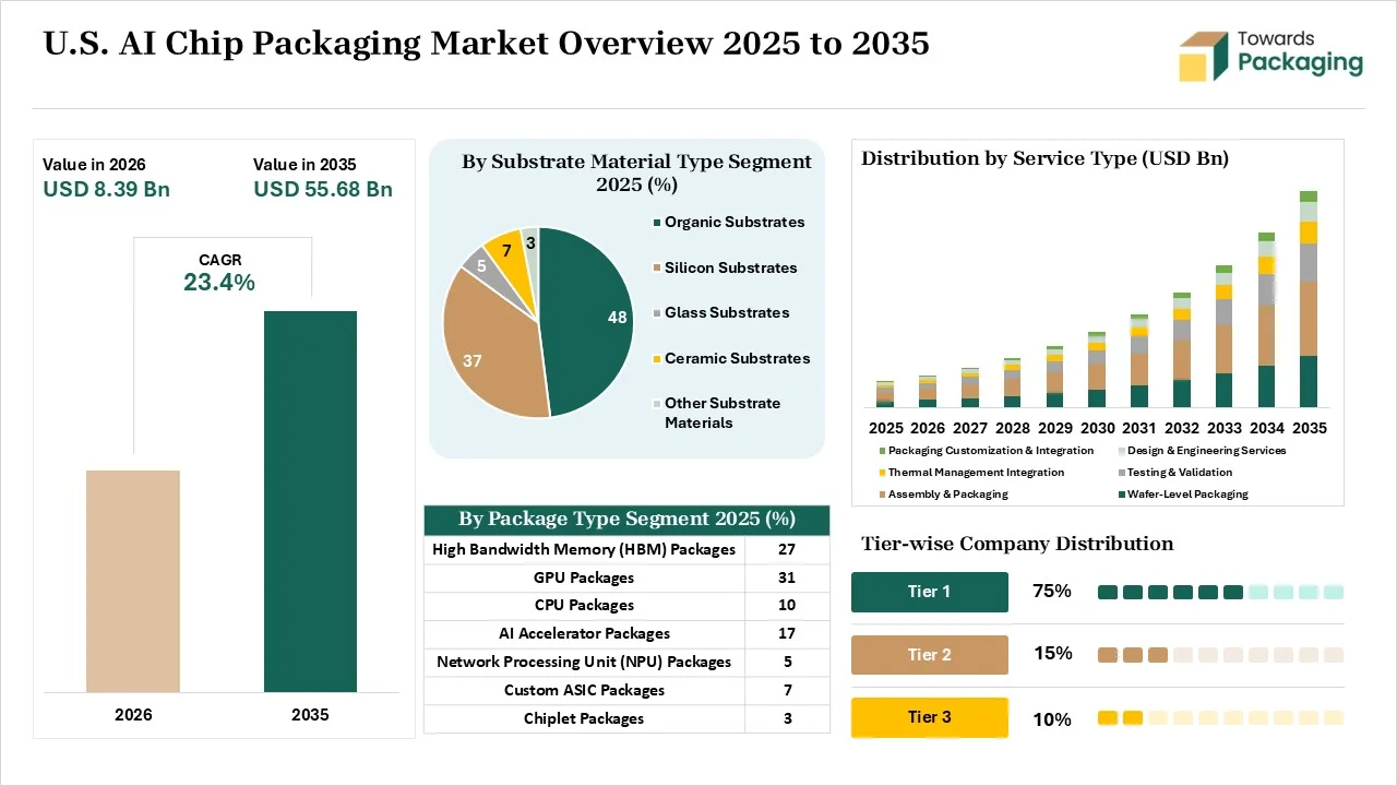
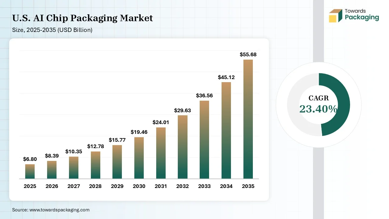
According to Vidyesh Swar, the U.S. AI chip packaging market size was estimated at USD 6.8 billion in 2025 and is predicted to increase from USD 8.39 billion in 2026 to approximately USD 55.68 billion by 2035, expanding at a CAGR of 23.40% from 2026 to 2035. Factors like the growing demand for Generative AI computing, expansion of chiplet-based architectures, growth in hyperscale data centers, presence of the CHIPS Act, proliferation of edge AI, expansion of hybrid bonding, innovations in autonomous systems, increased HBM integration, innovations in thermal management, and the burgeoning 3D stacking drive the market growth. Government funding for advanced packaging, the explosion of AI infrastructure, national security focus, and 5G telecommunication expansion increase demand for advanced semiconductor packaging.
| Market Value (2025) | USD 6.80 Billion |
| Forecast CAGR (2025-2035) | 23.40% |
AI chip packaging is the process of enclosing memory units and semiconductor dies in a single system. The packaging matters due to the shorter travel distances, better energy use, and high-speed communication. The core technologies in the architectural integration are chiplets, 2.5D packaging, and 3D stacking. The core interconnect technologies are TSV, CoWoS, and EMIB. The power delivery technologies are direct power channels and HBM. The benefits of AI packaging are low latency, energy efficiency, flexibility, and higher bandwidth. The structural components like HBM, diverse substrates, logic dies, and silicon interposers are required in AI chip packaging. The functionalities of AI chip packaging are yield control, heterogeneous integration, and shortening electrical pathways.
Advanced packaging overcomes the memory wall, integrates specialized mini-chips, offers better power control, and integrates 3D stacking in AI computing to accelerate data flow. The bandwidth innovations include reduced RC delay, short wire lengths, and higher pin counts, increasing demand for packaging. Factors like advanced cooling limits and reduced voltage swings increase demand for packaging. Technologies like hybrid bonding, interposers, TSV, and bridges are used in advanced packaging. Approaches like 3D stacking, thermal management, and 2.5D integration are used in advanced packaging.
Before the AI era, semiconductor firms in the United States focused on logic fabrication and developing front-end chips. Companies like IBM adopted interconnect concepts. The growing bandwidth limits in LLMs and deep learning increase demand for HBM integration and multi-chip design. Major American companies like Intel transition to 3D and 2.5D. AI accelerators increase demand for dense power delivery and new materials. The onshoring constraints in America increase the use of domestic-fabbed chips. In recent periods, advancements like power-delivery breakthroughs, domestic scaling, and innovative interconnects have increased the development of AI chip packaging.
The market includes technologies, package types, applications, substrate material, service, end users, and geographic areas. Technologies like 2.5D packaging, chiplet-based packaging, SiP, advanced wafer-level packaging, 3D packaging, fan-out packaging, flip-chip packaging, and other advanced packaging technologies are covered. Package types included are HBM packages, CPU packages, NPU packages, chiplet packages, GPU packages, AI accelerator packages, and custom ASIC packages. Applications covered include data center AI, HPC, automotive AI, telecommunications AI, defense & aerospace AI, generative AI, edge AI, consumer electronics AI, robotics & industrial AI. The substrate material like organic substrates, silicon substrates, glass substrates, and ceramic substrates, are included in the market. Services like wafer-level packaging, testing & validation, design & engineering services, assembly & packaging, thermal management integration, and packaging customization & integration are included. End users covered in the report are AI chip designers, IDMs, cloud service providers, automotive OEMs, research institutions, fabless semiconductor companies, hyperscale data center operators, system & server manufacturers, and defense & aerospace companies. The geographic areas like Western U.S., Southern U.S., Midwestern U.S., and Northeastern U.S. are covered in the market.
The increased training of advanced LLMs and the growing hyperscale investment increase the expansion of AI data centers. The focus on protecting local digital sovereignty and the limitations of monolithic processors increase the use of AI chip packaging. The deployment of server racks and the need to maximize computation increase the use of AI chip packaging. The rise in chip-level thermal management and the expansion of custom silicon strategies increase adoption of AI chip packaging. The expansion of U.S. AI data center infrastructure is a driver for market growth.
The need for high-precision interposers and expensive silicone interposers increases the cost. The use of precise structural materials and the utilization of microbumps increases the cost. The requirement for inorganic layers and failures of multi-die cascading increases the cost. The higher demand for advanced packaging materials and the higher tooling cost are responsible for the high cost. The extreme heat flux, low manufacturing yields, and stringent packaging interfaces in thermal materials increase the cost. The high cost of advanced packaging materials is a restriction for market growth.
The growing specialized neural processing and the development of custom silicon increase the manufacturing of custom AI chip packaging. The major cloud companies and the 5G infrastructure expansion increase the development of custom AI chip packaging. The need for high-bandwidth memory and the shift away from expensive single chip develops custom packaging development. The growing custom workloads and the rise in flexible building help with the growth. The expansion of custom AI packaging creates an opportunity for market growth.
The collaborations between chip designers, packaging vendors, semiconductor manufacturers, and government bodies help in the development of AI chip packaging.
The private investments of a billion dollars increase the expansion of AI chip packaging. The domestic production capacity is limited and supports Intel Foundry operations. The planned projects are developing TSMC Arizona, enhancing Nokia Allentown, and expanding Amkor Arizona. The region focuses on increasing regional capacity. It supports heterogeneous integration and chiplet partitioning.
| Parameters | Western U.S. | Southern U.S. | Northeastern U.S. | Midwestern U.S. |
| Major Production Hubs | Arizona, California |
Texas | New York | Ohio |
| Core Focus | Research & Development, Fabless AI Chip Architecture, 2.5D/3D Packaging Innovation |
Mainstream Packaging Lines, High-Volume Foundry Manufacturing |
Specialized Silicone Photonics, Defense-Aerospace Packaging Alliances |
Specialized Thermal Processing, Foundational Electronic Substrates |
Government initiatives like the CHIPS and Science Act help boost semiconductor production capacity. Partnerships like TSMC & Amkor Collaboration and strategic partnerships between Amkor and Nvidia scale advanced packaging. Intel Foundry Scaling supports increasing local advanced packaging.
In July 2026, the U.S. Department of Commerce launched a $140M initiative for developing wafer-scale systems and advanced chip packaging. The department plans to invest in Multibeam and focuses on manufacturing energy-efficient computing technologies. The advanced chip packaging is suitable for HPC systems, chiplets, and AI.
It is an advanced chip design that supports side-by-side placement of semiconductor chiplets. The architecture involves an interposer layer, micro-bumps, and through-silicone vias. The primary advantages are lower cost, high bandwidth, and better heat control. It is widely used in heterogeneous integration, AI accelerators, and high-performance computing. Its interposer base is made up of glass, silicone, and organic material
It is a microelectronics design that mounts multiple semiconductor chips vertically. It performs vertical stacking through TSVs. It uses hybrid bonding and handles physical anchoring. It is widely used in artificial intelligence, HPS, HBM, and consumer devices. It offers benefits like a smaller footprint and higher speed. Its main challenges include high cost, heat dissipation, and manufacturing stress. The thermal limitations are increased thermal resistance, hotspot amplification, high power density, and systemic thermal coupling.
It is a modular chip design method that offers key features like advanced interconnects, modular building blocks, and heterogeneous integration. It offers benefits like design flexibility, better manufacturing yields, and cost efficiency. It is widely used in automotive electronics, data centers, and artificial intelligence accelerators. The architecture includes modular partitioning, non-uniform access, and die-to-die interfaces.
The 2.5D packaging segment dominated the market with a 38% share in 2025. The rise in horizontally connected smaller chiplets and the focus on avoiding thermal dissipation challenges increase the use of 2.5D packaging. The growing demand for high-bandwidth connections and the focus on high energy efficiency increase adoption of 2.5D packaging. The expansion of data center accelerators and the presence of TSMC CoWoS platforms increase the use of 2.5D packaging. The presence of NVIDIA drives segment growth.
According to my research, the chiplet-based packaging segment held a 16% market share in 2025 and is expected to grow at the fastest CAGR of 30.20% during the forecast period. The focus on minimizing chiplet manufacturing cost and the need to enhance complex AI hardware increase the use of chiplet-based packaging. The growing node optimization and massive data transfer increase the use of chiplet-based packaging. The heterogeneous integration, faster data movement, and design flexibility in chiplet-based packaging support the segment growth.
The silicon interposer segment dominated the market with a 34% share in 2025. The growing large language model training and the rise in ultra-dense interconnects increase the use of silicon interposers. The need to lower structural warping and the rise in flexible functional blocks increase the use of silicon interposers. The low latency, high interconnect density, and ultra-dense wiring of silicon interposers drive the segment growth.
The hybrid bonding segment held a 10% market share in 2025 and is expected to grow at the fastest CAGR of 35.10% during the forecast period. The growing copper-to-copper connections and the modernization of AI workloads increase the use of hybrid bonding. The increased adoption of chiplet design and the rise in domestic fabrication increase the use of hybrid bonding. The rise in local advanced packaging helps with the expansion. The high density, direct connections, and reduced latency of hybrid bonding support the segment growth.
The GPU packages segment dominated the market with a 31% share in 2025. The growing generative AI workloads and the advancements in 2.5D packaging increase the use of GPU packages. Maximization of memory bandwidth and the rise in high-end accelerator platforms increase the use of GPU packages. The use of GPUs in generative AI training and the focus on preventing data delays increases the use of GPU packages, driving the segment growth.
The AI accelerator packages segment held a 17% market share in 2025 and is expected to grow at the fastest CAGR of 27% during the forecast period. The development of high-performance clusters and the growing domestic packaging foundries increases the use of AI accelerators. The presence of advanced 3D architectures and the concentration of cloud giants like Google increases the production of AI accelerator packages. The high power delivery and chiplet integration in AI accelerators support the segment growth.
According to my research, the data center AI segment dominated the market with a 52% share in 2025. The increasing use of specialized data chips and the transition to 3D packaging formats increase the use of AI chip packaging. The increased investment in the development of AI-based data centers and the rise in custom accelerators increase the adoption of AI chip packaging. The large-scale training and the growing system-level scaling drive the segment growth.
The generative AI segment held a 14% market share in 2025 and is expected to grow at the fastest CAGR of 29.70% during the forecast period. The need for immense computing power and the interest in advanced packaging materials increase the use of AI chip packaging. The requirement for thermal dissipation materials and the rise in multi-die complexity increase adoption of AI chip packaging. The growing liquid cooling integration and complex physical layouts in generative AI support the segment growth.
The organic substrates segment dominated the market with a 48% share in 2025. The expansion of high-frequency transmission and the focus on fine-pitch connections increase the use of organic substrates. The rise in flip-chip architecture and the expansion of standard fabrication processes increase adoption of organic substrates. The requirement for dense electrical connections and multi-chip stacking increases adoption of organic substrates. The manufacturing maturity and cost efficiency of organic substrates drive the segment growth.
The glass substrates segment held a 5% market share in 2025 and is expected to grow at the fastest CAGR of 33.50% during the forecast period. The rise in large-size chip designs and the need for clear signals in data transfer increases the use of glass substrates. The growing HPC training and the limitations on plastic base warp increase the use of glass substrates. The high electrical performance, superior thermal stability, larger form factors, and signal integrity of glass substrates support the segment growth.
According to my research, the thermal interface materials segment dominated the market with a 25% share in 2025. The high generation of heat flux and the transition to 2.5D chiplets increase the use of thermal interface materials. The focus on handling high thermal densities and the interest in premium thermal compounds increases the use of thermal interface materials. The complex architectures, high power density, and material innovation in thermal interface materials drive the segment growth.
The other packaging materials segment held a 5% market share in 2025 and is expected to grow at the fastest CAGR of 27.50% during the forecast period. The generation of advanced thermal interface materials and the interest in low-dielectric resins increase the use of other packaging materials. The expansion of AI packages and the dependence on encapsulation compounds increases adoption of other packaging materials. The shorter interconnects, advanced bonding, and extreme heat loads in advanced packaging materials support the segment growth.
The assembly & packaging segment dominated the market with a 34% share in 2025. The increased cost of single-die transistors and the massive data transfer increase the use of assembly & packaging. The explosion of high-density AI chips and the dependence on high-bandwidth memory increase the use of assembly & packaging. The expansion of OSAT providers and the heavy AI workloads increase the use of assembly & packaging, driving the segment growth.
The thermal management integration segment held a 10% market share in 2025 and is expected to grow at the fastest CAGR of 32.50% during the forecast period. The burgeoning power loads and the transition to vertical 3D stacking increase adoption of thermal management integration. The dependence on embedded cooling features and TIMs helps with the expansion. The rising heat loads and the onshoring initiatives require thermal management integration. The hotspot suppression, preemptive design, high power, and innovative cooling in thermal management integration support the segment growth.
According to my research, the AI chip designers segment dominated the market with a 28% share in 2025. The growing software-hardware integration and the rise in the fabless business model increase the use of AI chip packaging. The growing extreme bandwidth demands and the development of smaller modular chiplets increase the use of AI chip packaging. The need for higher electrical management and logic design expansion drives the overall segment growth.
The hyperscale data center operators segment held a 12% market share in 2025 and is expected to grow at the fastest CAGR of 27% during the forecast period. The development of ASICs and the rise in the combination of compute chiplets increase the use of AI chip packaging. The need to improve usable compute capacity and the rise in next-gen packaging help with the expansion. The rise in parameter sizes in LLMs and performance optimization demand support the segment growth.
Western U.S. focuses on power-delivery pathways and thermal management advancements. The regional packaging companies use EMIB technology and focus on R&D. The advanced innovations are electron-beam lithography platforms and co-packaged optics in the region. Companies like Intel and Nvidia develop AI accelerators and focus on other innovations. The region primarily focuses on AI architectural design.
The region's manufacturing capabilities focus on the supply of specialized equipment and HBM production. The presence of the SK Hynix Plant in Indiana increases the production of HBM chips. The region is equipped with strong logistical networks, smart factory lines, and advanced semiconductor facilities for the production of AI chip packaging. Opportunities like Intel’s Ohio Fab, lab-to-fab shift, and smart mobility demand support the semiconductor supply-chain expansion.
The presence of domestic fabrication pipelines in New Mexico and the availability of affordable land increase the development of AI chip packaging facilities. The presence of advanced facilities like Dallas & Houston operations and the Wistron Fort Worth Plant helps with the expansion. The major corporate investments and reliable power grids in these regions support the growth.
The presence of research institutions like Northeastern University, Penn State University, NEMC Hub, and MIT Lincoln Laboratory helps in R&D of AI chip packaging. Defense applications like tactile networking, missile guidance, electronic warfare, and C5ISR use AI chip packaging. Material innovations like 3D stacking, CPO, ultra-low-loss dielectrics, and ferroelectric memory support the market growth.
According to my research, the market is evolving rapidly, driven by the expansion of the domestic footprint of major companies. The leading semiconductor manufacturers include Amkor Technology and Intel Foundry helps in expanding local packaging capacity. The major OSAT company in the region is Amkor Technology. The major substrate providers are TTM Technologies and Intel Corporation. The specialized material companies are DuPont, Applied Materials, and Lam Research. The transition to 3D or 2.5D architectures drives the intense competition. Data Center AI holds the dominant position in the market due to the growing compute integration, rise in yield optimization, and the need for extreme compute density. The leading manufacturers are Amkor Technology, Micron Technology, Applied Materials, Intel Corporation, GlobalFoundries, and Cerebras Systems.
| Company Name | Technology Portfolio | AI Ecosystem Relationships | Geographic Presence | Innovation Strength |
| Intel Corporation | EMIB, Foveros, TGV, EMIB-T |
For simulation of chip design, the company uses Google Cloud. The company collaborated with Microsoft for AI capabilities. |
Santa Clara, California Hillsboro, Oregon Rio Rancho, New Mexico Folsom, California Austin, Texas Chandler, Arizona New Albany, Ohio San Jose, California Atlanta, Georgia |
Development of optical integration solutions, Adoption of glass substrate packaging |
| Amkor Technology | S-Connect, Heterogeneous Integration, Flip Chip Packaging, S-SWIFT |
The company partnered with Nvidia to create test technologies and advanced packaging. | Tempe, Arizona, West Chester, Pennsylvania |
Multi-Chiplet Architectures, High-Density Interconnects |
| Company Name | 2.5D Technologies | 3D Technologies | Hybrid Bonding Technology | Thermal Management Capabilities |
| Intel Foundry | EMIB, EMIB-M, EMIB-T, Foveros-S 2.5D, Foveros-R 2.5D, Foveros-B 2.5D |
Foveros Direct 3D, EMIB 3.5D, Intel 3-T |
Foveros Direct 3D | In-Package Liquid Cooling, Low Thermal Gradient Bonding |
| Amkor Technology | CoS, CoW, S-Connect, TSV Integration |
Stacked Die Processes, Advanced Wafer Handling, TSV |
Fine-Pitch Integration, 3D Die Stacking |
Thermal Test Measurement, Thermal Modeling and Simulation |
According to my research, the U.S. chip packaging market is expanding rapidly due to supply chain security, AI demand, and the transition to chiplets. 2.5D packaging is a major contributor to the market due to higher bandwidth, better scaling, shorter signal paths, and chiplet design. The silicon interposer is a key contributor to the market due to the burgeoning heterogeneous integration and the higher demand for thermal matching.
By Packaging Technology
By Interconnect Technology
By Package Type
By AI Chip Application
By Substrate Material
By Packaging Material
By Service Type
By End User
By Region



Principal Research Analyst
Vidyesh Swar is a Senior Research Analyst at Towards Packaging, bringing over 4 years of dedicated expertise in market intelligence and strategic analysis across the dynamic world of packaging technologies and solutions.
Learn more about Vidyesh Swar

Reviewed By
Aditi Shivarkar, with 14+ years in packaging market research, specializes in food, beverage, and eco-friendly packaging. She ensures accurate, actionable insights, driving Towards Packaging Analytics & Consulting 's excellence in industry trends and sustainability.
Learn more about Aditi Shivarkar


U.S. AI Chip Packaging Market
 Table of Content
 sales@towardspackaging.com
 +1 804-441-9344
 Download Sample
 Schedule a Meeting