 Market Overview 2025 to 2035")
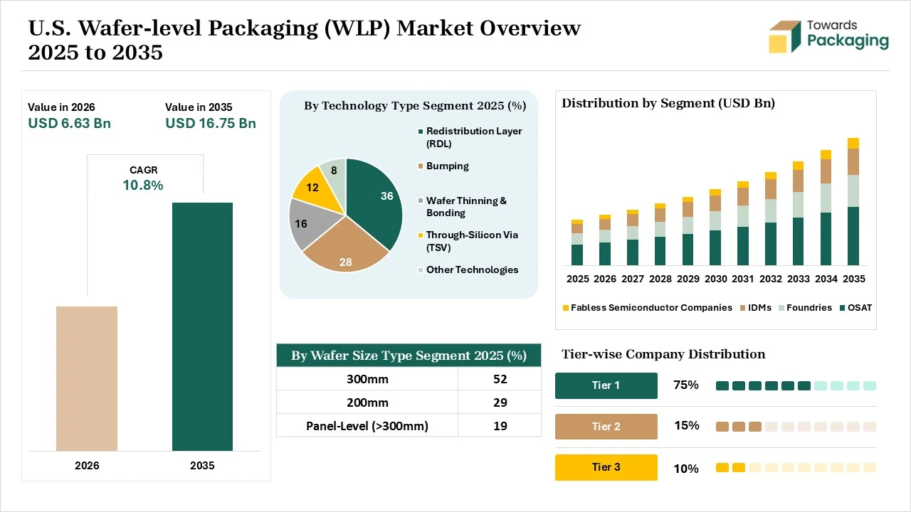
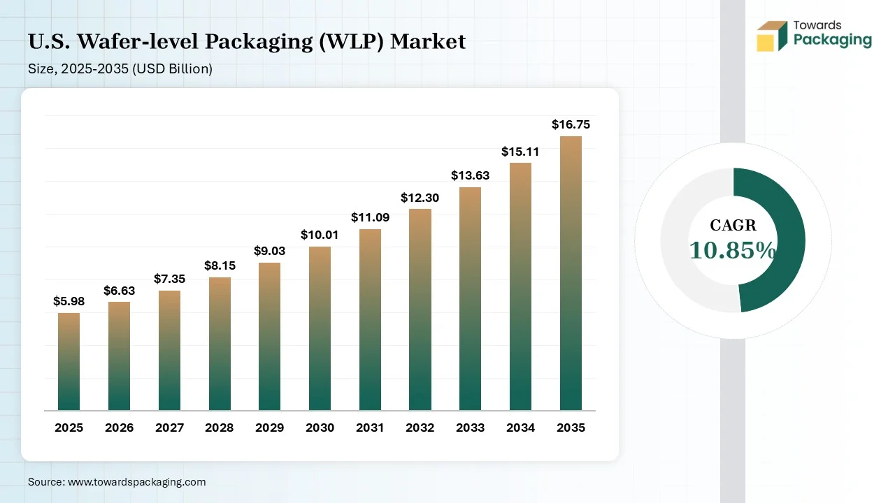
The U.S. wafer-level packaging (WLP) market is projected to grow from USD 6.63 billion in 2026 to USD 16.75 billion by 2035, registering a CAGR of 10.85%. The report provides detailed insights into market size, segment-wise analysis (fan-in WLP, fan-out WLP, and applications such as consumer electronics, automotive, and telecommunications), along with regional demand distribution across key U.S. states. It further includes comprehensive company profiling, competitive landscape assessment, value chain evaluation, and trade data analysis, along with manufacturers and suppliers data, offering a complete industry outlook.
 Market Size 2025 to 2035")
Wafer level packaging (WLP) is a high-level technology that counts the procedure of packaging as an integrated circuit (IC) is placed directly at the wafer level, resisting the regular procedure of packaging and assembling of every individual component. Such a strategy enables the manufacturing of semiconductor devices that are not only smaller and thinner but also more effective in terms of energy consumption and performance. The importance of WLP in the semiconductor sector cannot be overhyped, as it plays an important role in developing the complete result of the electronic devices while simultaneously lowering the production cost and minimizing the space demand.
AI has been contributing to the market with its integrative and high-skilled potential, which ensures intense thermal load handling. The unification of robust 2.5D/3D chiplets is highlighting the power of AI in the market. The valuable transitions in the autonomous vehicle infrastructure and 5G are driving the need and expansion of this robust technology, serving as a fuel to the transformation. The critical testing of infinit6e I/O contacts in a single packaging requires high-level tech attention to the testing and packaging, as well as to confirm safe use in the semiconductor sector.
Alongside, the AI chips need modernized packaging for connecting memory and compute strongly for excellent results. AI acts as a product and solution in this market, as it also elevates the design process and material development for the brand new semiconductor features that demand smart intervention with the tech-driven solutions. The diversified role of AI is a never-ending benefit to the market.
The AI-assisted inspection underlines the efforts of the manufacturers in utilizing the power of AI tools to develop precision in the modern packaging production space, mainly for the critical processes like TSV and fan-out.
Robust advancements in the U.S. WLP are the unification of heterogeneous chiplets, which allows various specialized chiplets to fit in a single package smoothly. This is a perfect integrative idea for AI and HPC. The extension of hybrid bonding lines stimulates the performance of connections that cooperate with the packaging strength. The rapidly rising automotive sector is attracting electrifying revenue for the U.S. WLP industry growth. The commendable processes, such as cooling channels, are a one-stop solution for either utilizing modern TIMs or equipping the direct packaging.
The spectacular status and innovations in the regional semiconductor sector demand packaging accordingly. The modernized interconnect schemes, like copper-to-copper direct hybrid bonding, call for strong WLP. The innovative materials are introduced to balance the warpage frequency in thin packages. While the advanced 3D packaging is serving the specialized techniques like PECVD and TSVs. The tech drive approaches is an automation boon for the critical packaging lines.
Market Size
Market Volume
As packaging urges are continuous, developing, the partnerships within the high-level packaging space are complicated. It’s crucial to communicate during the engagement and supply chain with users to completely understand their product and to be aware of their trends and developments. Involvement in consortium activities assists in showing and understanding where the sector is currently going because inventions are not being driven by one user, but rather the sector or market segment. Wafer-level packaging technology enables chips to continue to shrink in size, optimize production, and provide convenient ways to test chip functionality.
Fan-Out WLP (FO-WLP) segment dominated the market with 62% in 2025, and it is also expected to grow at the fastest CAGR of 12.80% during the forecast period. This packaging develops the regular WLCSP by allowing a huge number of input/output (I/O) links that expand beyond the die’s actual dimensions. This is completed with the assistance of a procedure that distributes the I/O pads across a huge area by using a restructured wafer procedure. FO-WLCSP is particularly beneficial for uses that require high I/O density, such as innovative mobile processors and automotive electronics, as it serves perfect electrical dependency and results while tracking an adjustable design.
The Fan-In WLP (FI-WLP) segment held 38% market share in 2025 as it is a tailored form of wafer level packaging where the input/output I/O) pads are kept inside the die footprint. Such a technique includes redistributing the pads to a hygiene pitch, which is followed by the usage of solder bumps to discover electrical links. Such a method is specifically advantageous for uses that require less package size and height, which makes them particularly suitable for handheld and mobile devices. In this packaging, once any wafer has completed testing and is launched to the packaging flow, a sputtering procedure begins to make a thin metal film layer.
The redistribution layer segment dominated the market with 36% share in 2025. As in current semiconductor packaging, redistribution layer technologies have played an important role in allowing smooth power distribution and signal routing inside the IC. With the assistance of a matched selection of RDL technologies, producers are receiving greater results and developing working integration in semiconductor packaging. The ideal package designer machine will enable us to effectively use the routing needs of the redistribution layer and update thermal management and signal integrity.
The wafer thinning and bonding segment held 16% market share in 2025 and is expected to have the fastest CAGR of 12.90% during the forecast period. Wafer thinning is important for manufacturing adjusted, high-performance semiconductors, and developing device reliability and effectiveness. The main procedure for wafer thinning is chemical-mechanical planarization and grinding, as it delivers different advantages in the thinning procedure. Thinning develops heat management, as it lowers chip stress, and develops packaging and dicing yield, which solves the complicated industry challenges. In semiconductor manufacturing, a crucial step is wafer thinning, which involves removing material from the wafer’s backside to achieve a particular thickness.
The through-silicon via (TSV) segment held the 21% market share in 2025, as such technology is utilized as an alternate choice to wire-link and flip chips (usually utilized in 2D IC packaging technology to make 2.5D and 3D packages and 3D IC. One of the initial benefits of TSV technology is its potential to develop data transfer rates for the chips. With regular interconnections in terms of 2D ICs, data signals pass through in parallel with the assistance of the silicon substrate, resulting in longer signal propagation delay.
The bumping & copper pillar segment held the 27% market share in 2025, because at its crucial point, copper pillar bumping is a procedure that is used to make electrical links in integrated circuits (ICs). The procedure includes saving copper columns, or pillars, in terms of a semiconductor wafer. Such pillars are then coated with a thin layer of solder or other conductive materials, which enables the link of the IC to a substrate or another chip. The accurate geometric designs of copper pillars invest in their admirable result characteristics, which make them an attention-grabbing selection for different uses.
The 300mm segment dominated the market with 52% share in 2025 because the transformation to 300mm Sic wafer design matches high-level packaging materials that have top-edge semiconductor fabrication and wafer-vel packaging procedure that develops current sector infrastructure and toolsets. This allows for repeat, big-volume production while assisting cost scaling and ecosystem compatibility. Additionally, the 300 mm design enables fabrication of bigger heat spreader components and interposers, which assist the sector’s course towards excessively bigger package design factors and more complicated heterogeneous assemblies.
Panel-Level ( >300mm) segment held the 19% market share in 2025, and it is also expected to grow at the fastest CAGR of 14.70% during the forecast period. It uses rectangular panels as an organic substitute, which is crafted particularly for high-volume manufacturing. Such an inventive strategy develops smoothness, lower costs, and discovers the flexibility of SiP and MCM assembly. By developing a simplified procedure, operating with known products, and transforming product functionality with accurate available technology for every needed function, as PLp serves different values and results.
The 200 mm segment held the 29% market share in 2025, as one crucial reason that 200mm fabs stay central for the semiconductor sector is their maturity. Such fabs have worked for many years, with highly updated procedure control, huge, updated machines, and constant equipment. Due to this, utilization rates at several 200mm availabilities are constantly between 80% and 100%, which showcases a rigid urge for mature procedure that nodes between 28nm and 90nm.
The consumer electronics segment dominated the market with 41% share in 2025 because semiconductors are basic in leveraging a multitude of technological machines across sectors, from medical equipment to smartphones. Such materials, with elements between conductors and insulators, perform important functions like energy conversion and signal amplification. The current invention in semiconductor technology develops smaller and more rigid chips that affect economic health worldwide.
The automotive electronics segment held the 19% market share in 2025, and it is also expected to grow at the fastest CAGR of 13.60% during the forecast period. Wafer-level packaging 9WLP) is a complicated approach for current automotive electronics, that delivers the miniaturization, high-speed data transmission, and thermal stability that are needed for electric and autonomous vehicles. Like regular methods, WLP packages have the complete silicon wafer before dicing, which results in a footprint that is approximately similar to the die size.
The industrial electronics segment held the 11% market share in 2025, because regular IC packaging includes storing specific chips into a printed circuit board (PCB) to link them electrically and serve physical protection. Hence, as chip complications develop, regular packaging procedures struggle to manage the rising number of I/Os (Input/Output) and dispel heat smoothly.
AWLP includes a series of inventive procedures that solve the restrictions of regular packaging methods. It includes the necessary packaging stages directly on the wafer before dicing it into particular chips.
The telecommunications segment held the 18% market share in 2025, as 5G technology develops ultra-low lag-time, huge device connectivity, and bandwidth. Acquiring such things needs standard semiconductor elements like baseband processors, RF chips, modems, and network processors. Semiconductors are materials that are generally made of silicon, which have electrical conductivity between insulators and conductors. They are utilized to produce microprocessors, integrated circuits, (ICs), sensors, and memory chips that develop almost every electronic device currently.
The OSAT (Outsourced Semiconductor Assembly & Test) segment dominated the market with 46% share in 2025 because companies carry a complicated position in the semiconductor value chain, which serves as support for production assistance for chip manufacturers. Their initial role is to serve third-party IC packaging and the official testing service, which ensures that silicon gets suspended after fabrication and is shifted into complete functional semiconductor elements that are set for integration into electronic machines. OSAT delivers characteristics as tailored links that allow the large-scale manufacturing of relevant semiconductor products.
The foundries segment held the 25% market share in 2025, and it is also expected to grow at the fastest CAGR of 12.60% during the forecast period. Wafer-level packaging plays a crucial role in the current miniaturization of passive elements, which serves substantial advantages in terms of performance, size, and cost. As the electronics sector continues to encourage the limitations of what is capable, wafer-level packaging will unquestionably stay at the forefront of inventions, which allows the making of more effective electronic machines.
IDM (Integrated Device Manufacturers) segment held the 29% market share in 2025, as semiconductor advanced packaging plays an important role in making electronic devices that align with the performance, power, and functionality demands of urgent environments. Such an atmosphere ranges from aerospace and defense to AI-driven communications and the automotive systems, which need microelectronics that are not only faster and smaller but also are thermally secured and effective.
The United States wafer-level packaging industry is constantly at the forefront of invention, which is being driven by the unlimited urge for compact and high-performance semiconductor machines. There is accelerated acceptance of 3D Integration and Heterogeneous Stacking, which is driven by the demand for greater results and energy efficiency. 3D stacking technologies are predicted to account for over 35% of developed revenue development. It allows technologies that count advanced die bonding machines and through-silicon vias (TSVs) and high-level die bonding machines.

By Packaging Type
By Technology
By Wafer Size
By Application
By End-User:

Research & Advisory Analyst
Yogesh Kulkarni is an experienced Research Analyst specializing in the packaging sector, with a strong foundation in statistical analysis and market intelligence. He currently contributes his expertise to Towards Packaging.
Learn more about Yogesh Kulkarni
Reviewed By
Aditi Shivarkar, with 14+ years in packaging market research, specializes in food, beverage, and eco-friendly packaging. She ensures accurate, actionable insights, driving Towards Packaging Analytics & Consulting 's excellence in industry trends and sustainability.
Learn more about Aditi ShivarkarU.S. Wafer-level Packaging (WLP) Market