


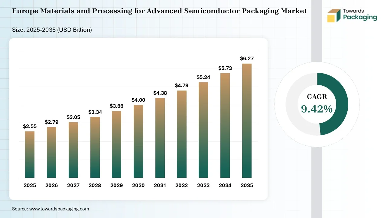
According to Vidyesh Swar, who is a specialist in fields like packaging materials, advanced packaging, and conventional packaging. The Europe materials and processing for advanced semiconductor packaging market size was $2.55B in 2025 and is predicted to reach $6.27B by 2035. The market is expected to grow at a 9.42% CAGR during the forecast period. Factors like the European Chips Act, expansion of IC substrate facilities, and demand for energy-efficient devices drive the overall growth. Companies like STMicroelectronics, ams OSRAM, AT&S, Infineon Technologies, and Soitec support the overall growth.
Materials and processing for advanced semiconductor packaging is the process of interconnecting multiple integrated circuits into high-performance electronics. Its core materials are substrates, interconnecting materials, thermal interface materials, encapsulants, dielectrics, interposers, and polymers. The processing steps include RDL formation, bump formation, singulation, die assembly, underfill dispensing, encapsulation, and final testing. Its benefits are enhanced performance, improved thermal management, miniaturization, and low power consumption. Its applications are HPC, 5G, machine learning, autonomous systems, and telecommunications.
Chiplet packaging, advanced substrates, and hybrid bonding are transforming the processing and materials needs in the Europe semiconductor packaging. The growing electric vehicles and miniaturization of electronic devices help with expansion. The region has a strong presence in industrial and automotive semiconductors. Austria is expected to grow with the fastest CAGR of 10.25% during the forecast period.
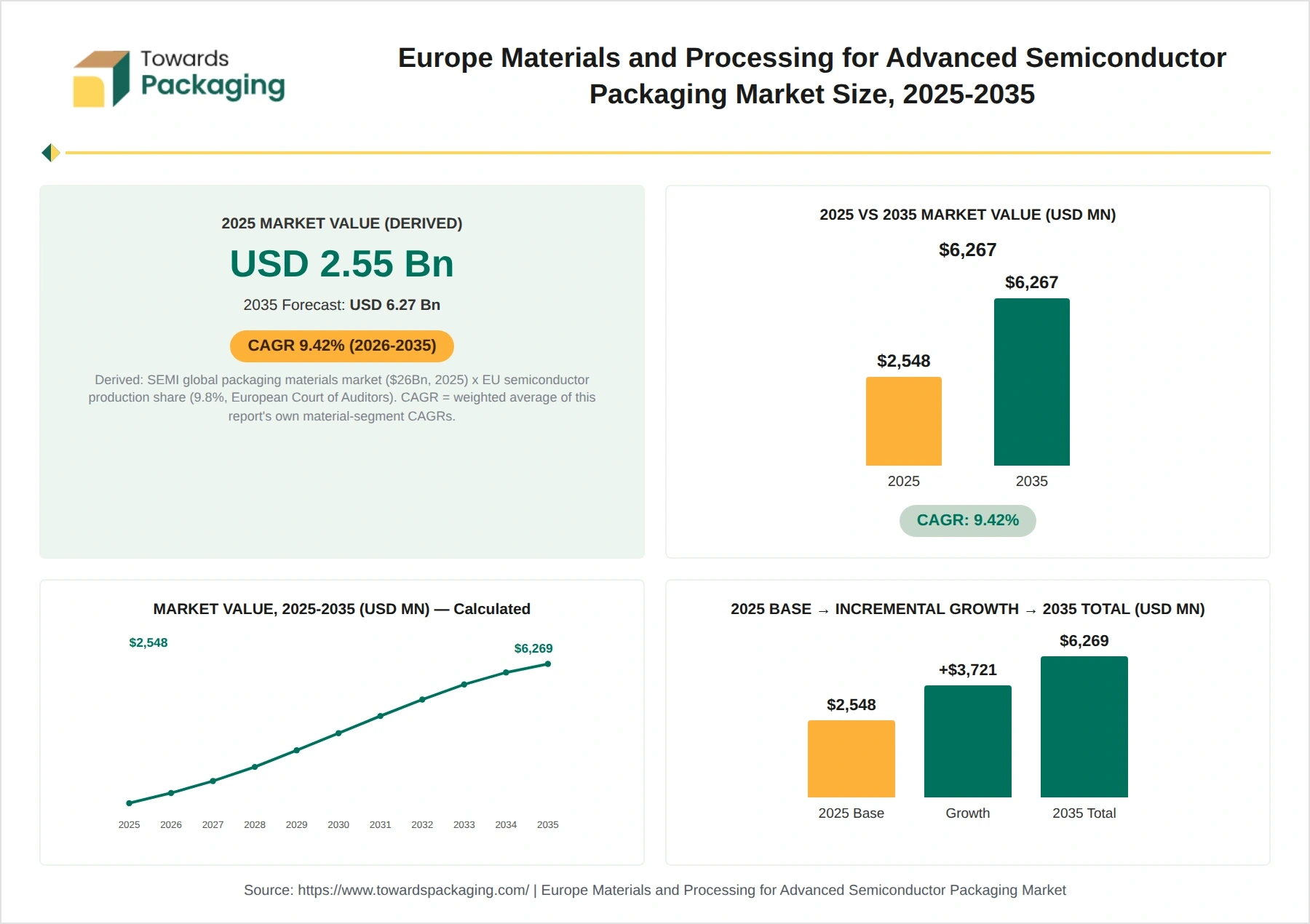
Europe materials and processing for advanced semiconductor packaging market size was estimated at $2.55B in 2025 and is expected to grow at the fastest CAGR of 9.42% during the forecast period. Growth factors like electrification of the automotive industry, rise in heterogeneous integration, demand for thermal management, expansion of telecom infrastructure, the EU Chips Act, interest in lighter electronic devices, and surge in high-performance computing help drive expansion. Major market players like Infineon Technologies, Soitec, AT&S, STMicroelectronics, and Robert Bosch support the overall growth.
The market is expected to reach $6.27B by 2035. The incremental growth of the market is $3.721B. Factors include the rise in public-private funding, consumers' EV transition, increased industrial automation, rising HPC demand, increasing chiplet adoption, a surge in energy-efficient processing, adoption of functional safety standards, expansion of domestic fabrication, and miniaturization of portable electronics, which will support the growth. Companies like EV Group, Infineon Technologies, ASML Holding N.V., and ASM International will contribute to the growth.
Source: SEMI Global Semiconductor Packaging Materials Outlook; European Court of Auditors; calculated compounding
Source: Towards Packaging Analytics & Consulting
Advanced substrates dominated the Europe materials and processing for advanced semiconductor packaging industry with a 27.65% share in 2025. The development of smart car systems and the interest in long-lasting chips increase the use of advanced substrates. The low dielectric constants, budget-friendly manufacturing, and performance balance of advanced substrates drive the growth. Thermal interface materials are expected to grow with the fastest CAGR of 12.20% in the market during the forecast period. The rise in electric vehicle production and focus on energy-efficient digital ecosystems increases use of thermal interface materials. The transition to advanced packaging architectures and surging HPC supports the overall growth.
Source: Towards Packaging Analytics & Consulting
Flip-chip packaging dominated the Europe materials and processing for advanced semiconductor packaging industry with a 20.30% share in 2025. The shift to ADAS and the presence of smart processing factories increase the use of flip-chip packaging. The high use of miniaturized devices in industrial IoT helps with expansion. The exceptional electrical performance and supply resilience of flip-chip packaging drive the growth. Chiplet packaging is expected to grow with the fastest CAGR of 15.05% during the forecast period. The large automotive base and the local manufacturing of semiconductor increases use of chiplet packaging. The scaling of 5G infrastructure and increased industrial automation increases the use of chiplet packaging, boosting the overall growth.
Source: Towards Packaging Analytics & Consulting
Encapsulation dominated the Europe materials and processing for advanced semiconductor packaging industry with a 13.25% share in 2025. The focus on protecting sensitive electronic systems and the growing industrial machinery automation increase the use of encapsulation. The focus on the safety of aerospace parts and high e-mobility demand drives the overall growth. Hybrid bonding is expected to grow at a 14.38% CAGR during the forecast period. The increased use of miniaturized chips in industrial automation and advanced packaging ecosystems increases the use of hybrid bonding. The low electrical resistance and direct copper connections in hybrid bonding support the overall growth.
Source: Towards Packaging Analytics & Consulting
Automotive electronics dominated the Europe materials and processing for advanced semiconductor packaging industry with a 26.40% share in 2025. The demand for advanced power electronics in the automotive sector and the domestic automotive manufacturing base increase the use of advanced semiconductor packaging. The presence of tier-1 car makers and a surge in battery management systems drives the overall growth. AI & high-performance computing is expected to grow with the fastest CAGR of 13.95% during the forecast period. The high requirements for HBM and the demand for high-reliability power electronics increase the use of advanced semiconductor packaging. The high use of multi-chip configurations and the high heat generation in AI chips boost the overall growth.
Source: Towards Packaging Analytics & Consulting
Integrated device manufacturers dominated the Europe materials and processing for advanced semiconductor packaging industry with a 31.50% share in 2025. The focus on long-term reliability of power electronics and limited OSAT infrastructure increases the use of advanced semiconductor packaging. Companies like NXP & Infineon, and interest in mixed-signal semiconductors drive the growth. Fabless semiconductor companies are expected to grow at an 11.70% CAGR during the forecast period. The modular interfaces of fabless firms and the presence of advanced material processors increase the use of advanced semiconductor packaging. Increased 3D stacking in fabless semiconductor companies and a strong telecommunications industry boost the overall growth.
Source: Towards Packaging Analytics & Consulting
Germany
Germany dominated the Europe materials and processing for advanced semiconductor packaging market with a 29.85% share in 2025. The presence of massive car manufacturers like Mercedes-Benz and the development of specialized power electronics increase the use of materials and processing for advanced semiconductor packaging. The advanced research infrastructure and focus on building local factories help with expansion. The engineering expertise and high-reliability microcontrollers drive the growth. Germany is expected to hold a 28.40% share by 2035. Factors like the rie in factory automation, focus on automotive-grade qualifications, and factory digitalization support the growth.
France
France held the second-largest share of 14.20% in the market in 2025. The focus on domestic semiconductor supply and surging EV production increases the use of advanced semiconductor packaging. The presence of high-performance technology and advanced research institutions drives the growth. France is expected to hold a 14.65% share in the market by 2035 due to the growing public-private investments. The transition to smart power semiconductors and manufacturing expertise boosts the overall growth.
Netherlands
Netherlands held a 12.65% share in the market in 2025. The strong foundation for heterogeneous integration and a surge in 5G connectivity increase the use of advanced semiconductor packaging. The interest in high-purity advanced materials and strong transport networks supports the growth. Netherlands is expected to hold a 12.95% share by 2035 due to a high-reliability automotive base. The high requirements for power electronics, HPC expansion, and surging tech demand boost the overall growth.
Austria
Austria held an 8.95% share in the market in 2025 and is expected to grow at the fastest CAGR of 10.25% during the forecast period. The focus on boosting local advanced packaging capabilities and the development of panel-level packaging helps with expansion. The rise in artificial intelligence processors and burgeoning advanced device miniaturization drives the growth. Austria is expected to hold a 10.20% share by 2035 due to the strong presence of IC substrates. The opening of wet-processing labs, increased sensor specialization, and surging AI demand boost the overall growth.
United Kingdom
The United Kingdom held an 8.55% share in the market in 2025. The growing chiplet architecture innovations and surge in autonomous vehicles increase the use of advanced semiconductor packaging. The government's focus on domestic semiconductor capacity and the rise in 3D integrated circuits boost the overall growth. United Kingdom is expected to hold an 8.75% share by 2035 due to specialized material innovation. The established advanced material fabrication, optimization of local chips, and miniaturization of advanced devices drive the growth.
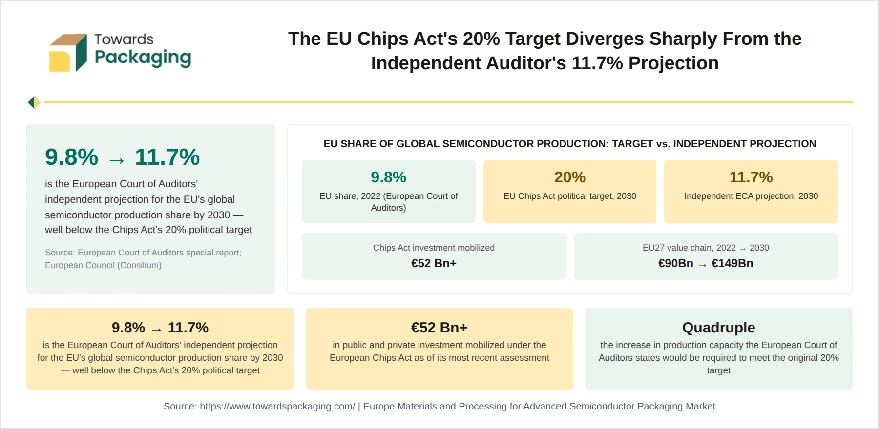
Source: European Court of Auditors; European Council (Consilium); European Commission
European Union held a 9.8% share in global semiconductor production. The independent European projection is 11.7% by 2030. European Union focuses on reaching a 20% share by 2030. The EU is doubling its chip production by 2030. It focuses on advanced chip manufacturing. In 2023, the EU invested €52B+ in the development of fabrication plants. The increased semiconductor production capacity needs to meet the original 20% target. The EU27 semiconductor value chain is expected to reach €49B by 2030. The strengths of the EU are R&D, design, equipment, and manufacturing base.
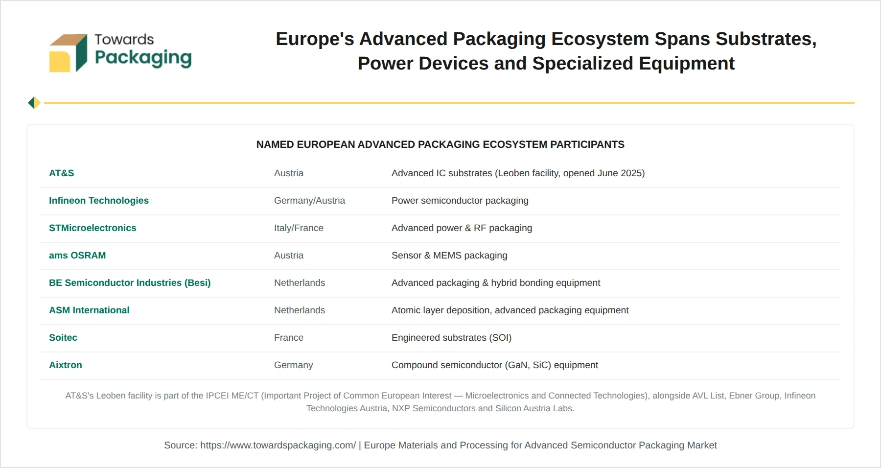
Source: Company disclosures (AT&S, Infineon, STMicroelectronics, ams OSRAM, Besi, ASM International, Soitec, Aixtron)
AT&S
The company’s headquarters are located in Leoben, Austria. The company offers products like HDI PCBs, SLP, IC substrates, specialized PCBs, and flexible PCBs. They offer technologies like embedded component packaging and power packaging. In June 2025, AT&S opened an advanced IC substrates facility in Leoben, Austria.
Infineon Technologies
The headquarters is located in the Germany and product range includes power management, microcontrollers, radio frequency devices, and security solutions. The company specializes in power semiconductor packaging. Its packaging contribution includes eWLB, AI power delivery modules, and DDPAK.
STMicroelectronics
The company is located in France and offers products like microcontrollers, MEMS, power transistors, industrial ICs, microprocessors, and other products. The company specializes in RF packaging and advanced power packaging.
ams OSRAM
The Austria-based company provides products like sensor solutions, interfaces, specialty lamps, LEDs, lasers, and photodetectors. The company specializes in MEMS and sensor packaging.
BE Semiconductor Industries
The Netherlands-based company specializes in hybrid bonding equipment and advanced packaging. They offer packaging equipment like singulation systems, molding systems, and trim systems.
ASM International
The Netherlands-based company specializes in advanced packaging equipment and atomic layer deposition. The core products include PECVD, epitaxy systems, vertical furnaces, and LPCVD.
Soitec
The France-based company provides engineered substrates. The key offerings include FD-SOI, POI, Power-SOI, RF-SOI, SmartSiC, and Photonics-SOI. They provide smart stacking and Smart Cut Technology.
Aixtron
The Germany-based company offers compound semiconductor equipment. They offer G10 Series, AIX 2800G4-TM, and AIX Planetary Reactor. The provides Epitaxy leaderships and wide-bandgap materials.
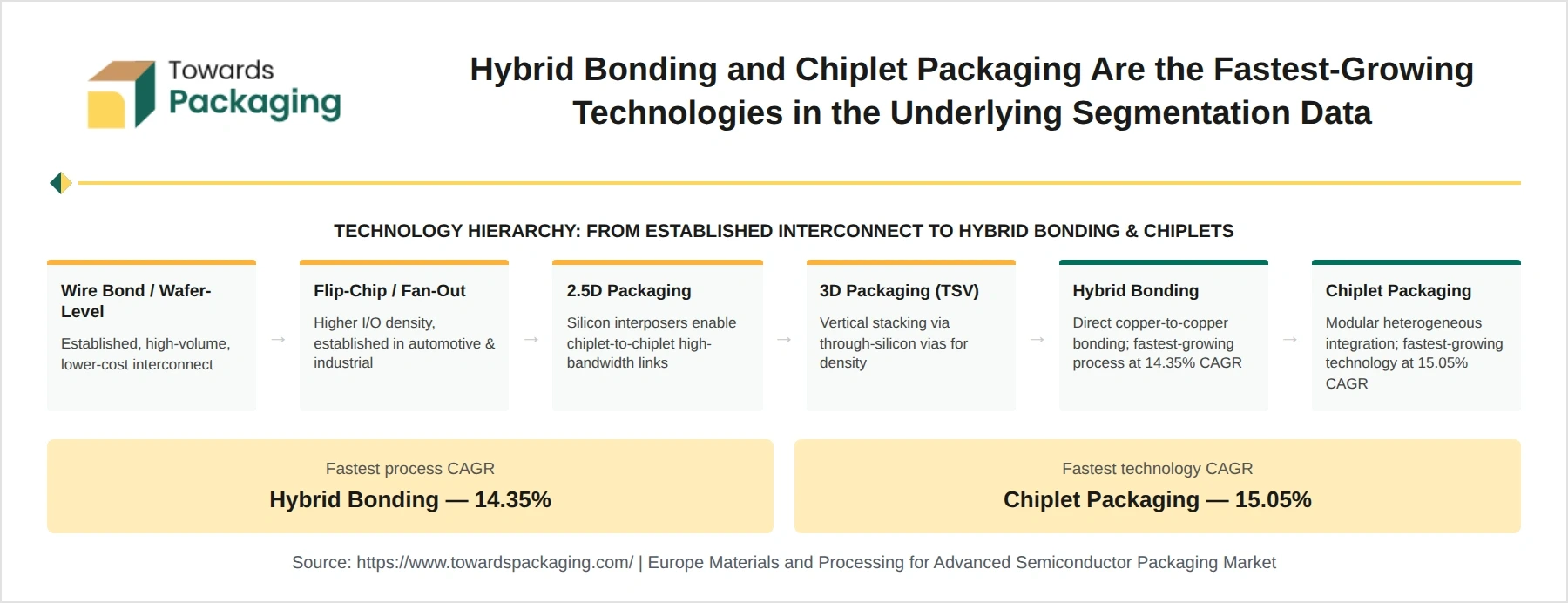
Source: Synthesis of this report's own segmentation data with general advanced-packaging technology literature
Wafer-Level Packaging
It is classified into Fan-Out WLP and Fan-In WLP. Its main benefits are low cost and ultra-compact size. Wafer-level packaging key innovations are heterogeneous integration, advanced redistribution layers, temporary bonding, and 3D integration.
Flip-Chip Packaging
Flip-chip packaging process steps are wafer bumping, flipping, reflow, and underfilling. Its benefits are higher density, better cooling, shorter paths, and smaller size. Key innovations include advancing underfill materials and hybrid bonding integration.
2.5D Packaging
2.5D packaging offers faster speed, supports easy cooling, and uses less power. It supports high-bandwidth memory integration and has high flexibility. It is widely used across data centers and artificial intelligence.
3D Packaging
3D packaging offers benefits like energy efficiency, faster speed, and higher density. The innovation includes advanced interposers, multi-material prototyping, sensor integration, and wafer-level integration. It is used in AI accelerators, smartphones, and HBM.
Hybrid Bonding
Hybrid bonding process methods are chip-to-wafer and wafer-to-wafer. They have direct copper contact, dielectric bonding, and do not have solder bumps. Their benefits are high density, better stacking, and faster speed. The key technological innovations are bump-less interconnects and the scaling of ultra-fine pitch.
Chiplet Packaging
Chiplet packaging is created using mixed technologies and offers excellent reusability. The common bonding methods are embedded bridges, 3D stacking, and hybrid bonding. The key innovations are advanced thermal management and standardized interconnects.
| Economic Indicator | Value | Context |
| Besi FY2025 gross margin | 63.30% | Disclosed gross margin for hybrid bonding and die-attach equipment, an indicator of pricing power in advanced packaging equipment |
| Besi FY2025 revenue | €591.3 million | Slight year-on-year dip masking a strong H2 2025 recovery driven by AI-related orders |
| Besi H2 2025 order growth | +63.6% vs. H1 2025 | Order backlog surge attributed to early HBM4 production-line bookings |
Source: BE Semiconductor Industries (Besi) FY2025 investor disclosure (published February 2026)
BE Semiconductor Industries' gross margin for FY205 is 63.3% for products like die-attach equipment and hybrid bonding. The key drivers for gross margins are advanced packaging solutions and stable manufacturing costs. The company generated annual revenue of €591.3 million in 2025. The revenue decreased slightly from 2024. The growth drivers for revenue are advanced packaging demand and the growing AI-related applications. The company’s H2 order growth is 63.6%. The rise in 2.5D packaging, photonics recovery, and popularity of hybrid bonding drives the H2 order growth.
| Metric | Value | Context |
| Global packaging equipment market (front-end) | $8 Bn+ | Front-end-related packaging equipment spending surpassed traditional back-end assembly for the first time in 2024 |
| Global packaging equipment market (back-end) | $7 Bn+ | Traditional back-end assembly equipment spending |
| Total global packaging equipment market | $15 Bn+ | Combined front-end and back-end packaging equipment spending, reflecting growing front-end/back-end convergence |
| EU Chips Act front-end-oriented investment | 10 of 13 confirmed/paused/cancelled FOAK projects | SEMI Europe's Chips Act Report finds Europe has so far prioritized front-end manufacturing investment over back-end/packaging capacity |
Source: IMAPS/3D InCites industry trade publication, citing BESI investor materials (March 2026); SEMI Europe Chips Act Report
The global front-end packaging market is valued at $8B+. Factors like burgeoning high-performance computing and advanced chip architectures drive the front-end packaging market growth. The global back-end packaging equipment market is valued at $7B+. Factors like the move to advanced packaging, government incentives, and innovative bonding technologies support the growth of the back-end packaging equipment market. The total global packaging equipment market is valued at $15B+. The e-commerce expansion, pharmaceutical demand, and utilization of advanced robotics boost growth. The total 13 FOAK projects are under the EU Chips Act. This act gives preference to front-end manufacturing investment. 4 FOAK projects are approved under the EU Chips Act.
| Value-Chain Stage | Named European Example |
| Materials (substrates, underfills, TIMs) | AT&S (Austria) - advanced IC and glass-core substrates |
| Process equipment (bonding, dicing, inspection) | BE Semiconductor Industries / Besi (Netherlands) - hybrid bonding and die-attach equipment; ASM International (Netherlands) - atomic layer deposition |
| Compound semiconductor equipment | Aixtron (Germany) - GaN/SiC equipment |
| Engineered substrates | Soitec (France) - silicon-on-insulator substrates |
| R&D / pilot-line integration | Fraunhofer-Gesellschaft (Germany), CEA-Leti (France), imec (Belgium), VTT (Finland) - EU Chips Act pilot-line consortium members |
| Device packaging (power/RF/sensor) | Infineon Technologies (Germany/Austria), STMicroelectronics (Italy/France), ams OSRAM (Austria) |
Source: Structural framework derived from this report's own Material Type and Process segmentation, illustrated with named company examples
Materials
The materials like organic substrates, dielectric materials, silicon, glass, tin-silver solder, underfill, thermal interface materials, silicone, copper, nickel, and EMC are required.
Process Equipment
Process equipment includes wafer dicing, stencil printing, flip-chip bonding, polymer dispensing, encapsulation, thermal curing, and cleaning.
Compound Semiconductor Equipment
It includes thinning systems, wet processing systems, underfill systems, encapsulation presses, thermal processing ovens, and electroplating systems.
R&D/Pilot-Line Integration
R&D focuses on thermal compression bonding, back-end convergence, PLP, and co-packaged optics.
Device Packaging
It includes wafer preparation, RDL formation, bumping, advanced interconnection, molding, and singulation.
| Technology Milestone | Detail | Date/Source |
| Fine-pitch die-to-wafer hybrid bonding | CEA-Leti demonstrated hybrid bonding down to 1 micron pitch for multi-die stacking integration | ECTC 2026 (April 2026 disclosure) |
| Hybrid bonding placement accuracy | Besi's latest-generation hybrid bonding systems offer 100 nanometer placement accuracy | Besi order announcement, May 2024 |
| Standardization of hybrid bonding + TSV | Fraunhofer IZM was the first organization in Europe to adopt hybrid bonding combined with through-silicon vias as its standard R&D approach, now industry-standard | Fraunhofer IZM |
| Automotive chiplet integration | imec's Automotive Chiplet Alliance focuses on wafer-to-wafer hybrid bonding research for automotive applications | imec |
| EU Chips Act packaging pilot lines | APECS (heterogeneous integration/chiplets), NanoIC (beyond-2nm), FAMES (low-power FD-SOI), PIXEurope (photonic ICs) | European Commission Chips Act pilot-line program |
Source: Fraunhofer IZM; CEA-Leti (ECTC 2026 conference disclosure, April 2026); imec; Besi/Applied Materials company disclosures
| Regulatory/Strategic Factor | Detail |
| EU Chips Act target vs. independent projection | 20% political target for EU global semiconductor production share by 2030, vs. 11.7% independent European Court of Auditors projection (up from 9.8% in 2022) |
| EU Chips Act investment mobilized | More than €52 billion in public and private investment (European Commission, Chips Act 2.0 proposal materials) |
| EU27 semiconductor value chain | €90 billion (2022) projected to grow to €149 billion by 2030 (European Council) |
| Dutch Vifo Act | The Netherlands' Investments, Mergers and Acquisitions Security Screening Act is the primary regulatory hurdle for foreign acquisition of Dutch semiconductor equipment companies (e.g., Besi, ASML, NXP) |
European Chips Act vs. Independent Projection
European Chips Act is backed by planned investment of €43 billion. The target for global semiconductor production is 20% by 2035. The Act focuses on strengthening manufacturing innovation and research. The Act attracts new industry talent.
EU Chips Act Investment Mobilized
The total over €52 billion investment mobilized by the EU Chips Act. EU directly offered €3.3B from Digital Europe and Horizon Europe. The pillars of mobilization are research, manufacturing, and supply chain security. The key funding goals are to double the market share. The major funding channels are the Chips Fund and the Chips Joint Undertaking.
EU27 Semiconductor Value Chain
The value chain size was estimated at €90 billion in 2022. The market is projected to reach €149B by 2030. It focuses on industrial, power semiconductors, and automotive chip applications. The initiative focuses on enhancing domestic semiconductor manufacturing capacity.
| Organization | Type | Country | Core Focus |
| AT&S | Industrial company | Austria | Advanced IC substrates, glass-core substrates |
| Infineon Technologies | Industrial company | Germany/Austria | Power semiconductor packaging |
| STMicroelectronics | Industrial company | Italy/France | Advanced power & RF packaging |
| ams OSRAM | Industrial company | Austria | Sensor & MEMS packaging |
| BE Semiconductor Industries (Besi) | Industrial company | Netherlands | Hybrid bonding & die-attach equipment |
| ASM International | Industrial company | Netherlands | Atomic layer deposition, packaging equipment |
| Soitec | Industrial company | France | Engineered substrates (SOI) |
| Aixtron | Industrial company | Germany | Compound semiconductor (GaN, SiC) equipment |
| Fraunhofer-Gesellschaft (incl. IZM, FBH, IHP) | Research institute | Germany | APECS pilot-line coordinator; hybrid bonding + TSV standardization |
| CEA-Leti | Research institute | France | FAMES pilot-line coordinator; fine-pitch hybrid bonding (1 micron demo) |
| imec | Research institute | Belgium | NanoIC pilot line; Automotive Chiplet Alliance |
| VTT | Research institute | Finland | APECS & NanoIC pilot-line partner |
| TU Graz | Research institute | Austria | APECS pilot-line partner |
| FORTH | Research institute | Greece | APECS pilot-line partner |
| IMB-CNM, CSIC | Research institute | Spain | APECS pilot-line partner |
| INL | Research institute | Portugal | APECS pilot-line partner |
| Tyndall National Institute | Research institute | Ireland | NanoIC pilot-line partner |
Source: Company disclosures (Besi, AT&S, Applied Materials); EU Chips Act pilot-line consortium disclosures (Fraunhofer, CEA-Leti, imec, VTT); European Court of Auditors; European Council
| Company | Product Portfolio Focus |
| AT&S | Advanced IC substrates; glass-core substrates for AI, HPC, and photonics (in development, per April 2026 company disclosure) |
| Besi | Hybrid bonding systems (100nm placement accuracy); die-attach equipment |
| ASMPT | Thermo-compression bonding (TCB) equipment; second-generation hybrid bonding equipment |
| Soitec | Silicon-on-insulator (SOI) engineered substrates |
Source: AT&S company disclosures; Besi company disclosures
| Company | Product Portfolio |
| AT&S |
|
| Besi |
|
| ASMPT |
|
| Soitec |
|
| Country | Named Organizations Present | Role in Ecosystem |
| Germany | Fraunhofer-Gesellschaft (incl. FBH, IHP), Infineon Technologies, Aixtron | APECS pilot-line coordinator; power packaging; compound semiconductor equipment |
| France | CEA-Leti, Soitec, STMicroelectronics | FAMES pilot-line coordinator; engineered substrates; power/RF packaging |
| Belgium | imec | NanoIC pilot-line host; Automotive Chiplet Alliance |
| Netherlands | Besi, ASM International | Hybrid bonding and packaging equipment manufacturing |
| Austria | AT&S, ams OSRAM, TU Graz, Infineon Technologies Austria | Advanced IC substrate manufacturing (Leoben, opened June 2025); sensor/MEMS packaging; APECS partner |
| Italy | STMicroelectronics | Power/RF packaging |
| Finland | VTT | APECS and NanoIC pilot-line partner |
| Ireland | Tyndall National Institute | NanoIC pilot-line partner |
| Greece | FORTH | APECS pilot-line partner |
| Spain | IMB-CNM, CSIC | APECS pilot-line partner |
| Portugal | INL | APECS pilot-line partner |
Source: EU Chips Act pilot-line consortium disclosures (APECS, NanoIC, FAMES, PIXEurope); AT&S; Besi; Infineon; STMicroelectronics
Germany
The processing solutions like AIXTRON SE, Suss Microtec, and SCHMID are present in Germany. Materials suppliers like Siltronic AG, Henkel AG, and BASF SE are present. The research company Fraunhofer ASSID and Fraunhofer IZM is located in Germany. These companies' roles are specialty material supply, development of high-vacuum systems, and production of high-reliability parts.
France
Companies like STMicroelectronics, CEA-Leti, Soitec, and Tessalia are present in France. The companies focus on the development of specialized substrates, R&D collaboration, and supporting high-performance infrastructure.
Belgium
Research companies like imec, power packaging suppliers like MinDcet NV & CISSOID, and Material suppliers like Applied Materials & Fujifilm are present across Belgium. Belgian ecosystem focuses on pilot prototyping, fine-pitch interconnects, and dielectrics.
Netherlands
The equipment companies include ASM International, Sempro Technologies, Besi, and Boschman Technologies, which are present in the Netherlands. Material suppliers like Schunk Xycarb Technology and Fujifilm Electronic Materials are located in the Netherlands. The company's core focus is on heterogeneous integration and machinery innovation.
Austria
Companies like AT&S, Lam Research, Applied Materials Austria, EV Group, Besi Austria GmbH, and Silicon Austria Labs are present across Austria. The company focuses on wafer-bonding technologies and the development of high-end IC substrates.
According to my research, the Europe materials and processing for advanced semiconductor packaging market is expanding rapidly. Drivers like digital sovereignty, specialized thermal management demand across industries, green EU standards, and the move to electric vehicles drive the market growth. Germany held the highest share in the market, at 29.85% in 2025. The top players like BASF, ASML, NXP Semiconductors, Henkel, Dow Chemical, and Applied Materials contribute to the growth.
Our Experts
Vidyesh Swar researched the 2025 market value, forecast value, demand & supply analysis, regional analysis, and segmental share analysis.
Aman worked on the regulatory environment, technology & innovation, pricing analysis, competitive landscape, product portfolio, recent developments, and value chain analysis.
Aditi reviewed the entire report, corrected inconsistencies, identified errors, maintained quality standards, and make report-ready for publication.
By Material Type
By Advanced Substrate
By Processing Technology
By Process
By Application
By End User
By Country











Principal Research Analyst
Vidyesh Swar is a Senior Research Analyst at Towards Packaging, bringing over 4 years of dedicated expertise in market intelligence and strategic analysis across the dynamic world of packaging technologies and solutions.
Learn more about Vidyesh Swar

Reviewed By
Aditi Shivarkar, with 14+ years in packaging market research, specializes in food, beverage, and eco-friendly packaging. She ensures accurate, actionable insights, driving Towards Packaging Analytics & Consulting 's excellence in industry trends and sustainability.
Learn more about Aditi Shivarkar

Europe Materials and Processing for Advanced Semiconductor Packaging Market
 Table of Content

 Download Sample
 Schedule a Meeting