The through-silicon via (TSV) IC packaging market covers an in-depth evaluation of global market size, historical growth patterns, and future revenue projections supported by detailed statistical data. The report provides insights into major trends such as heterogeneous integration, 3D packaging adoption, chiplet architectures, and advancements in semiconductor materials. It includes segmentation by packaging type, materials, and end-use industries, along with regional coverage across North America, Europe, Asia-Pacific, Latin America, and the Middle East & Africa.
Additionally, it examines competitive dynamics, profiling top companies, analyzing market shares, reviewing value chain structures, and presenting international trade flows, import–export data, supplier networks, and manufacturing footprints.
The through-silicon via (TSV) IC packaging market refers to the sector involved in the manufacturing and adoption of packaging technologies for integrated circuits that use through-silicon via for electrical connections between multiple layers of semiconductor materials. TSV technology is essential in enabling high-density, high-performance, and low-power semiconductor devices. It is widely utilized in applications such as memory, imaging, communication systems, and mobile devices due to its ability to provide improved performance and miniaturization.
Through-silicon via IC packaging is an advanced semiconductor packaging technology that involves creating vertical electrical connections, or via, that pass completely through a silicon wafer or die. These vias allow multiple integrated circuit layers or dies to be stacked and interconnected directly, enabling three-dimensional (3D) integration. Unlike traditional wire bonding or flip-chip methods, TSV technology significantly reduces the length of interconnects, which improves electrical performance by lowering signal delay, power consumption, and heat generation. TSV IC packaging is widely used in applications requiring high performance and compact form factors, such as high-end smartphones, 3D memory, logic-memory integration, and advanced computing systems.
AI integration can significantly enhance the through-silicon via (TSV) IC packaging market by optimizing design, manufacturing, and testing processes. In the design phase, AI algorithms can rapidly simulate and predict the electrical and thermal behaviour of TSV structures, allowing engineers to develop more efficient and reliable chip layouts. During manufacturing, AI-driven analytics can monitor real-time data to detect defects early, improve wafer alignment accuracy, and reduce material waste, thereby enhancing production yield and cost-effectiveness.
AI can identify subtle anomalies and patterns that traditional methods may miss, ensuring higher reliability. Additionally, AI helps accelerate innovation by enabling predictive modelling and process automation, ultimately speeding up time-to-market for complex 3D ICs and chiplet-based systems. As the demand for high-performance and miniaturized electronics continues to grow, AI will play a crucial role in scaling TSV packaging to meet industry requirements with greater precision, efficiency, and adaptability.
Demand for Miniaturization and High-Performance Devices
As consumer electronics, especially smartphones, tablets, and wearables, continue to become thinner and more powerful, there is a rising need for compact semiconductor solutions. TSV technology enables vertical stacking of chips, reducing the package footprint while maintaining or improving performance, making it ideal for space-constrained designs.
Thermal Management Challenges in 3D Stacked Dies & Design Complexity and Limited Design Tools
The key players operating in the market are facing issues due to thermal management challenges in 3D stacked dies and design complexity, which is estimated to restrict the growth of the market. While TSVs offer improved performance, stacking multiple dies can lead to significant heat accumulation. Effective thermal dissipation remains a technical hurdle, particularly in densely packed, high-power applications, which can affect device reliability and lifespan.
Designing TSV-based ICs is significantly more complex than traditional packaging methods. Limited availability of mature design automation tools and modelling software for 3D integration adds to the design difficulty, slowing down the development cycle. The TSV fabrication process is sensitive and prone to defects such as misalignment, voids, or copper contamination. These defects can reduce production yields and increase wastage, affecting the overall profitability for manufacturers.
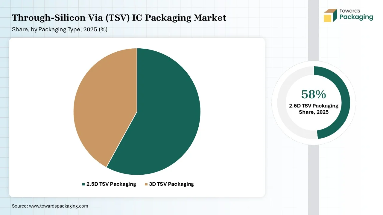
The 2.5D Through-Silicon Package (TSP) packaging segment is considered a dominant packaging type in the through-silicon via (TSV) IC packaging market due to its optimal balance between performance and cost-effectiveness. One of the main advantages of 2.5D TSP is its use of an interposer to connect multiple dies side by side, enabling high bandwidth, shorter interconnect lengths, and improved signal integrity while avoiding some of the thermal and manufacturing complexities of full 3D stacking. This makes it highly suitable for high-performance computing, GPUs, networking devices, and data center applications where speed, power efficiency, and miniaturization are critical. Additionally, it offers better thermal management and easier testing and debugging compared to 3D ICs. The growing demand for AI, IoT, and advanced networking is further fueling the need for high-speed and scalable solutions, making 2.5D TSP an attractive and widely adopted packaging choice.
 IC Packaging Market Share, by Packaging Type 2025 (%)")
The 3D through-silicon via (TSV) packaging segment is the fastest-growing segment in the through-silicon via IC packaging market due to its ability to deliver exceptional performance in compact form factors. This packaging technology enables vertical stacking of multiple dies with high-density interconnects, resulting in reduced signal delay, lower power consumption, and enhanced bandwidth. These benefits are critical for applications such as high-performance computing, advanced smartphones, AI processors, and data centers where space, speed, and energy efficiency are vital. Moreover, the increasing demand for miniaturized devices with greater functionality is accelerating the adoption of 3D TSV packaging across various high-end electronics sectors.
The silicon segment is the dominant material segment in the through-silicon via (TSV) IC packaging market due to its superior electrical, mechanical, and thermal properties that make it ideal for advanced packaging applications. Silicon is highly compatible with semiconductor manufacturing processes and offers excellent conductivity and heat dissipation, which are essential for high-density and high-performance integration. Its ability to support vertical interconnects through precise etching and filling techniques allows for efficient die stacking and signal routing in 2.5D and 3D TSV structures. Additionally, silicon interposers offer better structural integrity and reliability, which is crucial in mission-critical applications like high-performance computing, AI, and data centers. The widespread availability and mature processing infrastructure further strengthen silicon's position as the preferred material in TSV IC packaging.
The gallium arsenide (GaAs) segment is the fastest-growing material segment in the through-silicon via (TSV) IC packaging market due to its exceptional electronic properties that outperform traditional silicon in specific high-frequency and high-speed applications. GaAs offers higher electron mobility and greater resistance to radiation, making it ideal for radio frequency (RF) devices, satellite communications, radar systems, and advanced wireless technologies such as 5G. As demand rises for compact, power-efficient devices with superior signal performance, GaAs becomes increasingly preferred for its ability to maintain signal integrity and speed in harsh environments. Additionally, growing investments in aerospace, defense, and high-frequency telecom infrastructure are accelerating the adoption of GaAs-based TSV packaging, positioning it as a key growth driver in the advanced semiconductor materials landscape.
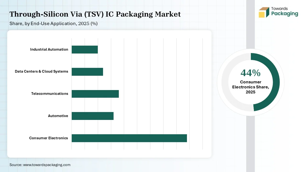
 IC Packaging Market Share, by End-Use Application Type 2025 (%)")
The consumer electronics segment is the dominant end-user application segment in the through-silicon via (TSV) IC packaging market due to the rising demand for high-performance, compact, and energy-efficient electronic devices. Modern consumer electronics such as smartphones, tablets, wearable devices, and gaming consoles require advanced packaging solutions that support high-speed processing, reduced latency, and enhanced functionality within smaller footprints. TSV technology enables vertical stacking of chips, which allows for increased device capabilities while minimizing size and power consumption. Additionally, rapid technological advancements and increasing consumer expectations for faster, smarter, and more efficient devices are driving manufacturers to adopt TSV packaging. The mass production of consumer electronics and the continuous innovation in product design further solidify this segment’s dominance in the TSV IC packaging market.
The automotive segment is the fastest-growing segment in the through-silicon via (TSV) IC packaging market due to the increasing integration of advanced electronic systems in modern vehicles. Technologies such as advanced driver-assistance systems (ADAS), autonomous driving, in-vehicle infotainment, and electric powertrains require high-performance, compact, and energy-efficient semiconductor solutions. TSV packaging enables faster data processing, reduced latency, and enhanced reliability, which are critical for safety and real-time decision-making in automotive applications. As the automotive industry shifts toward electrification and intelligent mobility, the demand for robust and high-density IC packaging solutions like TSV continues to surge, making the automotive segment a key growth driver in this market.
 IC Packaging Market Share, by Region Type 2025 (%)")
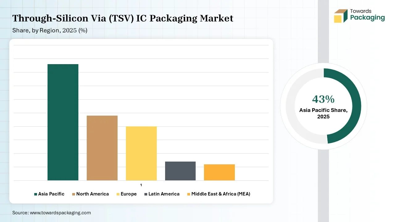
The Asia-Pacific region holds a dominant position in the through-silicon via (TSV) IC packaging market due to its well-established semiconductor manufacturing ecosystem, strong presence of foundries, and robust electronics production base. Countries like China, Taiwan, South Korea, and Japan are home to leading semiconductor companies and contract manufacturers, which drive the demand and development of advanced packaging technologies like TSV.
Asia Pacific benefits from cost-effective labor, a skilled workforce, and substantial investments in R&D and infrastructure by both the government and private sectors. Additionally, rapid adoption of cutting-edge technologies such as AI, 5G, IoT, and high-performance computing across consumer electronics and automotive sectors further fuels the need for TSV-based solutions. The growing demand for miniaturized, high-speed, and energy-efficient devices continues to strengthen Asia-Pacific’s leadership in this market.
China Market Trends
China plays a key role as a global manufacturing hub for electronics and semiconductors. The country is rapidly advancing its domestic semiconductor capabilities through government support, such as the "Made in China 2025" initiative. Its strong demand for consumer electronics, smartphones, AI devices, and electric vehicles fuels the adoption of TSV technology. China is also investing heavily in advanced packaging fabs and research institutions to reduce dependence on foreign chip technologies.
South Korea Market Trends
South Korea, led by tech giants like Samsung and SK Hynix, is a key player in TSV integration, particularly for high-bandwidth memory (HBM) used in high-performance computing and graphics. The country’s advanced infrastructure, significant R&D spending, and leadership in memory technologies position it strongly in the TSV segment. It also supports a robust supply chain for both logic and memory components using TSV packaging.
Japan Market Trends
Japan contributes to the TSV market through its expertise in precision equipment, materials, and semiconductor components. While it no longer leads in chip manufacturing, Japanese firms are instrumental in developing advanced packaging materials and tools essential for TSV fabrication. Its focus on high-reliability applications in automotive and industrial electronics supports stable demand for TSV integration.
India Market Trends
India is emerging as a promising market for semiconductor and advanced packaging development, driven by government initiatives like the “Semicon India Programme.” While its TSV infrastructure is still developing, the growing local demand for 5G, AI, and consumer electronics, combined with incentives for chip manufacturing, creates long-term potential for TSV technology adoption.
North America is witnessing rapid growth in the through-silicon via (TSV) IC packaging market, largely driven by the expanding adoption of advanced automotive electronics and electric vehicle (EV) systems. As EVs and autonomous vehicles require high-speed data processing, real-time decision-making, and compact power-efficient designs, TSV technology plays a crucial role in enabling high-performance computing and sensor integration within limited space. The region's strong presence of leading EV manufacturers, automotive technology firms, and semiconductor innovators supports this momentum. Furthermore, growing investments in automotive R&D, coupled with the push for energy-efficient and intelligent mobility solutions, are accelerating the adoption of TSV-based 3D ICs in vehicle systems.
U.S. Market Trends
The United States is the primary driver of TSV IC packaging adoption in North America, especially in automotive and electric vehicle technologies. Leading EV manufacturers like Tesla, along with strong semiconductor companies and R&D institutions, are pushing the integration of advanced 3D ICs using TSVs for high-performance computing in ADAS, battery management systems, and in-vehicle infotainment. Government incentives promoting clean energy and EV adoption, along with a robust ecosystem of automotive tech startups and chip designers, further support the growth of TSV solutions in automotive applications.
Canada Market Trends
Canada is contributing to the regional TSV market growth through its expanding electric vehicle industry and focus on sustainable automotive technologies. Government-backed clean mobility initiatives and partnerships with U.S.-based semiconductor and automotive firms are helping bring advanced packaging technologies into EV systems. While Canada has a smaller semiconductor manufacturing base, it is investing in R&D and smart mobility solutions that benefit from TSV-enabled compact and efficient ICs.
Europe is growing at a notable rate in the through-silicon via (TSV) IC packaging market due to its strong industrial focus on advanced automotive technologies, electrification, and semiconductor innovation. The region’s automotive giants are increasingly incorporating electric powertrains, ADAS, and connected vehicle systems, all of which require high-speed data transmission and compact chip designs that TSV packaging enables. Moreover, Europe’s push toward digital sovereignty and reduced reliance on foreign semiconductor supply chains has led to increased investments in domestic chip manufacturing and advanced packaging R&D. The growing integration of AI, IoT, and smart infrastructure applications across industries also supports TSV adoption.
 IC Packaging Market Companies")
By Packaging Type
By Material
By End-Use Application
By Region

Research & Advisory Analyst
Yogesh Kulkarni is an experienced Research Analyst specializing in the packaging sector, with a strong foundation in statistical analysis and market intelligence. He currently contributes his expertise to Towards Packaging.
Learn more about Yogesh Kulkarni
Reviewed By
Aditi Shivarkar, with 14+ years in packaging market research, specializes in food, beverage, and eco-friendly packaging. She ensures accurate, actionable insights, driving Towards Packaging Analytics & Consulting 's excellence in industry trends and sustainability.
Learn more about Aditi ShivarkarThrough-Silicon Via (TSV) IC Packaging Market