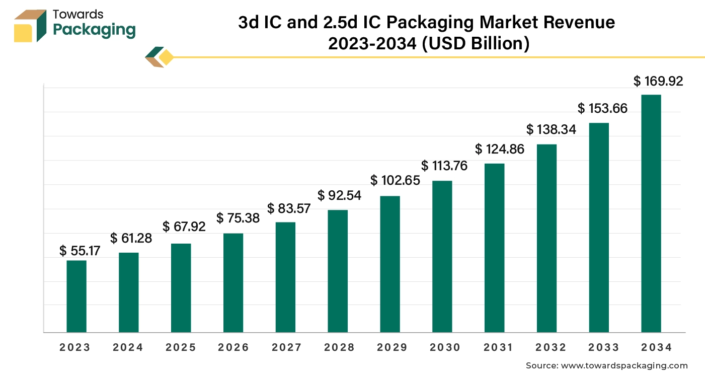
The 3D IC and 2.5D IC packaging market is forecasted to expand from USD 75.30 billion in 2026 to USD 190.29 billion by 2035, growing at a CAGR of 10.85% from 2026 to 2035. This report provides a detailed analysis of the market’s segmentation, including key packaging technologies such as WLCSP, TSV, and 2.5D. It also covers regional data, showcasing the dominance of Asia Pacific and the rapid growth expected in North America. The competitive analysis includes key players like Samsung, TSMC, and Intel, along with insights into manufacturers and suppliers. Additionally, the value chain and trade data are comprehensively examined to provide a complete market overview.

3D and 2.5 ICS offer a more compact form factor and minimize power consumption compared to traditional packaging methods, which is important for mobile gadgets and other space-constrained applications. The key players operating in the market are focused on adopting inorganic growth strategies like acquisition and merger to develop advance technology for manufacturing 3D IC and 2.5D IC packaging which is estimated to drive the global 3D IC and 2.5D IC packaging market over the forecast period.
The packaging technology of 2.5D and 3D is used to package several integrated circuits in one package. To achieve a very high die-to-die connection density, two or more active semiconductor chips are arranged side by side on a silicon interposer in a 2.5D configuration. Die stacking is used in 3D structures to incorporate active chips for the shortest connectivity and smallest package footprint. 2.5D and 3D have become more and more popular as the best chiplet integration* platforms in recent years because of their advantages in obtaining very high package densities and good energy efficiency.
The packaging technology of 2.5D and 3D are cutting-edge methods used to improve semiconductor devices' efficiency, functionality, and performance. In order to create a three-dimensional structure, many layers of silicon wafers or dies are stacked vertically in 3D IC packaging. Logic, memory, and analogue integrated circuits (ICs) can all be integrated into one package thanks to this stacking. allows for greater capability in a smaller package. Performance is improved via shorter interconnects between layers, which shorten the time a signal travels. It is possible to boost data bandwidth between components by stacking layers. The global packaging industry size is growing at a 3.16% CAGR.
3D IC packaging involves stacking multiple layers of silicon wafers or dies vertically, creating a three-dimensional structure. This stacking allows for the integration of different types of ICs (such as logic, memory, and analogue) within a single package.
2.5D IC packaging involves placing multiple dies side-by-side on a single interposer, which is a layer of silicon or other material that contains the interconnections between the dies. This creates a “half” 3D effect by arranging the dies horizontally and connecting them through the interposer.
| Metric | Details |
| Market Size in 2025 | USD 67.93 Billion |
| Projected Market Size in 2035 | USD 190.29 Billion |
| CAGR (2026 - 2035) | 10.85% |
| Leading Region | Asia Pacific |
| Market Segmentation | By Packaging Technology, By Application, By End User and By Region |
| Top Key Players | Samsung, Taiwan Semiconductor Manufacturing Company, Ltd. (TSMC), Intel Corporation, ASE Technology Holding Co., Ltd., Amkor Technology |
Artificial Intelligence can help find and create new materials that will improve IC packaging performance and dependability. Artificial Intelligence (AI) can find interesting candidates for novel materials by evaluating performance data and material attributes. The 3D and 2.5D IC packaging sector can achieve better performance, increased efficiency, and improved quality by utilizing AI, which will spur additional innovation and growth in this area.
AI algorithms can analyze and optimize the design of 3D and 2.5D ICs, improving performance, reducing power consumption, and minimizing thermal issues. AI can automate complex design tasks and find optimal configurations faster than traditional methods. AI can predict and identify potential yield issues in the manufacturing process by analyzing data from previous production runs. This helps in adjusting parameters to improve yield rates and reduce defects. AI-driven simulations can help in designing better thermal management solutions for 3D ICs. AI models can predict heat distribution and identify potential hotspots, leading to more effective cooling solutions.
By examining patterns in data from testing and inspection procedures, artificial intelligence (AI) can improve fault identification and diagnosis. This enhances dependability by making it possible to identify flaws and anomalies more quickly. The efficiency and precision of 3D and 2.5D IC testing and validation procedures can be improved by using artificial intelligence (AI).
Complex test data can be interpreted by AI algorithms, which can also verify that ICs fulfill performance and quality requirements. AI can improve production procedures in manufacturing by evaluating data from production machinery and sensors. This may result in decreased downtime, increased overall efficiency, and better process control.
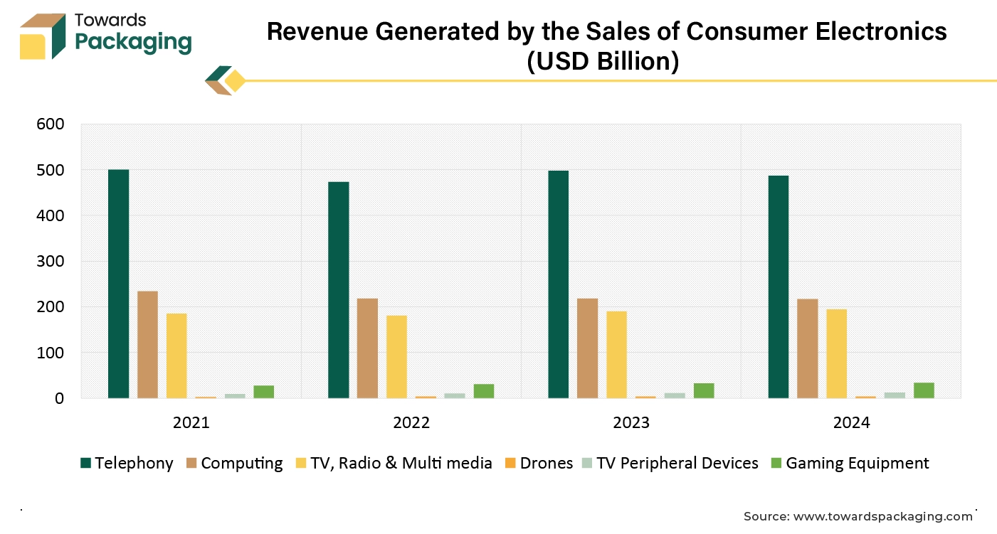
Rapid industrialization and urbanization has given boom to consumer electronics demand and encouraged the development of new gadgets to be used in day-to-day life. Continuous innovation in electronics leads to new and improved devices with enhanced features, performance, and capabilities. This drives consumers to upgrade to the latest technology. The increasing trend of streaming services, gaming, and other digital media expands the demand for high-quality consumer electronics like TVs, audio systems, and gaming consoles. The demand for smartphones, tablets, and other portable devices continues to grow as they become essential tools for communication, work, and entertainment. The proliferation of the Internet of Things (IoT) and smart devices has developed an expanding ecosystem of connected electronics, from smart homes to wearable technology, boosting demand.
Increased interest in smart home technologies, such as voice assistants, smart thermostats, and security systems, drives the demand for various connected devices. Expanding middle-class populations and improved infrastructure in emerging markets contribute to higher demand for consumer electronics as more people gain access to these technologies.

The key players operating in the market are facing challenges during manufacturing as well as reliability and yield concerns which is restricting the growth of the 3D IC and 2.5D IC packaging market. 3D and 2.5D IC packaging require expensive materials and technology, which may discourage adoption, particularly for businesses with limited resources.
The manufacturing of 3D and 2.5D integrated circuits (ICs) entails complex procedures like fine pitch interconnects and through-silicon vias (TSVs), which are difficult and demand sophisticated machinery. Controlling heat dissipation in closely spaced 3D integrated circuits is difficult and can have an impact on performance and dependability. It is a major engineering problem. Because of the intricacy of the 3D and 2.5D ICs, it can be challenging to achieve high yield and ensure long-term reliability.
Due to rapid development in automotive industry and aim to reduce CO2 emission, the electric vehicles are adopted by the most of the people. Smart infrastructure and smart city projects are increasingly becoming a focus for urban development and modernization. Advancing intelligent transportation systems (ITS) to improve traffic management, reduce congestion, and enhance public transportation through real-time data and connectivity.
The key players are engineering and ddeveloping smart grids to enhance the efficiency and reliability of electricity distribution, incorporating real-time monitoring and automated control systems to manage energy consumption. The key players operating in the market are focused on adopting inorganic growth strategies like partnership to develop smart infrastructure for electric vehicle charging on public streets which is estimated to create lucrative opportunity for the growth of the 3D IC and 2.5D IC packaging market over the forecast period.
For instance,
With Siemens' Innovator3D IC software, developing a digital twin of the entire semiconductor package assembly is made easier with a single data model for design planning, prototyping, and predictive analysis. The mechanical design, testing, signoff, implementation, multiphysics analysis, and release to manufacture are all guided by this cockpit. It facilitates quick "what-if" investigation while recognizing, averting, and resolving issues before the implementation of a thorough design by combining power, signal, thermal, and mechanical stress analysis methods. Subpar outcomes or expensive, time-consuming downstream rework can be avoided with this shift-left methodology.
| Rank | Company | Headquarters | Country | Why Relevant | Key Packaging Products/Services |
| 1 | TSMC | Hsinchu | Taiwan | Industry leader in advanced 2.5D and 3D packaging technologies | CoWoS, SoIC, InFO, advanced chiplet packaging |
| 2 | Samsung Electronics | Suwon | South Korea | Global leader in advanced semiconductor packaging and HBM integration | I-Cube, X-Cube, H-Cube packaging |
| 3 | Intel | Santa Clara, California | USA | Pioneer in heterogeneous integration and 3D chip stacking | Foveros, EMIB, advanced packaging |
| 4 | ASE Technology Holding | Kaohsiung | Taiwan | World's largest OSAT with comprehensive advanced packaging capabilities | VIPack, Fan-Out, SiP, 2.5D packaging |
| 5 | Amkor Technology | Tempe, Arizona | USA | Leading OSAT provider for advanced packaging and wafer-level solutions | Flip-chip, Fan-Out, 2.5D packaging |
| Rank | Company | Headquarters | Country | Why Relevant | Key Packaging Products/Services |
| 1 | JCET Group | Wuxi, Jiangsu | China | Major OSAT with growing advanced packaging capabilities | Fan-Out, SiP, advanced IC packaging |
| 2 | Powertech Technology | Hsinchu | Taiwan | Leading provider of memory and advanced packaging services | Memory packaging, TSV, HBM packaging |
| 3 | Tongfu Microelectronics | Nantong, Jiangsu | China | Expanding advanced packaging services for global semiconductor companies | Flip-chip, wafer-level packaging |
| 4 | SPIL | Taichung | Taiwan | Advanced IC assembly and testing services | Flip-chip, BGA, wafer-level packaging |
| 5 | Nepes | Asan | South Korea | Specialist in wafer-level and fan-out packaging technologies | Fan-Out, wafer-level packaging |
| Rank | Company | Headquarters | Country | Why Relevant | Key Packaging Products/Services |
| 1 | Deca Technologies | Tempe, Arizona | USA | Innovator in fan-out and adaptive patterning technologies | Fan-Out packaging platforms |
| 2 | Adeia | San Jose, California | USA | Develops IP for hybrid bonding and advanced packaging technologies | Hybrid bonding IP, 3D integration |
| 3 | Chipbond Technology | Hsinchu | Taiwan | Specialized provider of display driver and wafer-level packaging | COF, wafer bumping, advanced packaging |
| 4 | Unimicron | Taoyuan | Taiwan | Leading manufacturer of advanced IC substrates for 2.5D/3D packaging | ABF substrates, IC package substrates |
| 5 | Shinko Electric Industries | Nagano | Japan | Major supplier of advanced semiconductor package substrates | Flip-chip substrates, advanced package substrates |

The MEMS/Sensors segment accounted for a notable share of the 3D IC and 2.5D IC packaging market in 2025. MEMS and sensors often require integration with additional electronic components (e.g., signal processing units, power management circuits). 3D IC and 2.5D IC packaging enable compact, high-density integration, minimizing the overall footprint and supporting for more compact device designs. Microelectronics, microactuators, and microsensors are the functional parts of MEMS.
Accelerometers, gyroscopes, digital compasses, inertial modules, pressure, humidity, microphones, and smart sensors are a few examples of the sophisticated components of MEMS. MEMS and sensors often require integration with additional electronic components (e.g., signal processing units, power management circuits). 3D IC and 2.5D IC packaging enable compact, high-density integration, reducing the overall footprint and allowing for more compact device designs.
A compact design is essential to all of these components and sensors. As a result, a lot of sensors have begun using 2.5D and 3D IC packages. These benefits make 3D and 2.5D IC packaging particularly advantageous for MEMS and sensor technologies, where performance, size, and integration are critical. The key players operating in the market are focused on launching new MEMs/Sensors, which has observed to raise the demand for the 3D IC and 2.5D IC packaging and estimated to drive the growth of the segment over the forecast period.
For instance,
The consumer electronics segment registered its dominance over the global 3D IC and 2.5D IC packaging market in 2025. The rapid innovation in technology such as innovations and improvements in processing power, display quality, and connectivity (e.g., 5G), drives need for new and next generation electronic devices. The augmentation in adoption and innovation of smart devices, including wearables, smart home gadgets, and smart devices, is expanding the market as consumers seek integrated and connected experiences. Increasing advancement in wearable tech, such as fitness trackers and smartwatches, are creating new market segments and driving additional consumer interest.
For instance,
Asia Pacific region dominated the global 3D IC and 2.5D IC packaging market in 2025. Asia-Pacific region is home to leading semiconductor manufacturers and foundries, such as Samsung and Taiwan Semiconductor Manufacturing Company (TSMC). These companies are at the forefront of advanced packaging technologies, including 3D IC and 2.5D IC. The Asia-Pacific region benefits from lower production costs and a well-established supply chain, making advanced packaging technologies more economically viable for large-scale production. Many countries in Asia Pacific region are focused on developing smart city and smart infrastructure due to rise in adoption of the 3D IC and 2.5D IC packaging, which is estimated to drive the 3D IC and 2.5D IC packaging market over the forecast period.
For instance,
More than 89% of Japan's GDP is generated by the automobile industry. Japan is actually the third-biggest automobile manufacturer in the world! However, Japan has not embraced zero-emission vehicles (ZEVs) as quickly as several other Asian nations have. Japan's economic stability will be impacted by the success or failure of its automobile industry as the world transitions more quickly to ZEVs. This will have a big impact on Japan's still-emerging role in the changing global EV scene.
China 3D IC and 2.5D IC packaging market is driven by the robust foundry and OSAT Ecosystem and growing domestic demand, which has estimated to drive the growth of the 3D IC and 2.5D IC packaging market in the near future. “Made in China 2025” and other national strategies emphasize semiconductor self-sufficiency. Heavy investments through government funds (e.g., the China Integrated Circuit Industry Investment Fund) bolster R&D and manufacturing. The presence of major OSAT (Outsourced Semiconductor Assembly and Test) companies like JCET, Tongfu Microelectronics, and Tianshui Huatian Technology. These companies are rapidly adopting advanced packaging techniques including 2.5D/3D integration to compete globally. China has invested heavily in building a localized supply chain for substrates, bonding equipment, and packaging materials.
North America region is projected to host the fastest-growing 3D IC and 2.5D IC packaging market in the coming years. North America, particularly the U.S., is home to major technology and semiconductor companies like Intel, AMD, and NVIDIA, which are leading the development and adoption of advanced packaging technologies, including 3D IC and 2.5D IC. North America has a well-established ecosystem that includes leading packaging technology providers, material suppliers, and equipment manufacturers, which supports the growth and adoption of advanced packaging solutions.
Many North American companies are forming strategic partnerships and investing in advanced packaging technologies to gain a competitive edge and address evolving market needs. The region has a strong demand for high-performance computing solutions, including in data centers, AI applications, and high-end consumer electronics, which drives the need for advanced packaging to meet performance and power efficiency requirements.
")
Europe region is seen to grow at a notable rate in the foreseeable future. Europe invested heavily in semiconductor research through initiatives like Horizon Europe and public-private partnerships such as the European Processor Initiative and IPCEI (Important Projects of Common European Interest). Europe’s focus on electric vehicles, autonomous driving, and Industry 4.0 drives demand for high-performance, compact IC packaging solutions, including 2.5D and 3D ICs. European demand for energy-efficient and high-speed computing solutions encourages adoption of advanced IC packaging technologies.
In European countries, the manufacturing of 3d IC and 2.5D IC packaging is advancing as industries increasingly adopt semiconductor solutions. Nations like France, Germany, and the UK are at the forefront, driven by strong automotive, industrial automation, and user electronics sectors. Supportive initiatives such as the European Chips Act are further boosting research, development, and local manufacturing of advanced semiconductor packaging. Collaboration between leading companies and research institutions is accelerating innovation, with uses ranging from smart electronics to next-generation automotive systems.
In Latin America, the demand and production of 3D IC and 2.5D IC packaging are steadily gaining attention as industries shift toward advanced semiconductor technologies. The region is witnessing growing adoption in areas such as consumer electronics, telecommunications, IoT devices, and industrial automation, in which miniaturisation and high performance are important. Countries like Brazil are emerging as main hubs for adoption and localized production, while others in the region are also starting to discover opportunities in this space. Although still developing compared to global leaders, Latin America is showing strong capability, with increasing investments and interest driving the demand for compact, efficient, and next-generation electronic solutions.
In the Middle East and Africa, the demand and production of 3D IC and 2.5 IC packaging are starting to gain attention, specifically in regions pushing toward more compact and high-performance electronic systems. In Saudi Arabia, industry stakeholders recognize the value of these advanced packaging technologies, especially for applications demanding high integration density, enhanced processing power, and smooth form factors -making them increasingly complicated for electronics manufacturers and emerging semiconductor ventures.
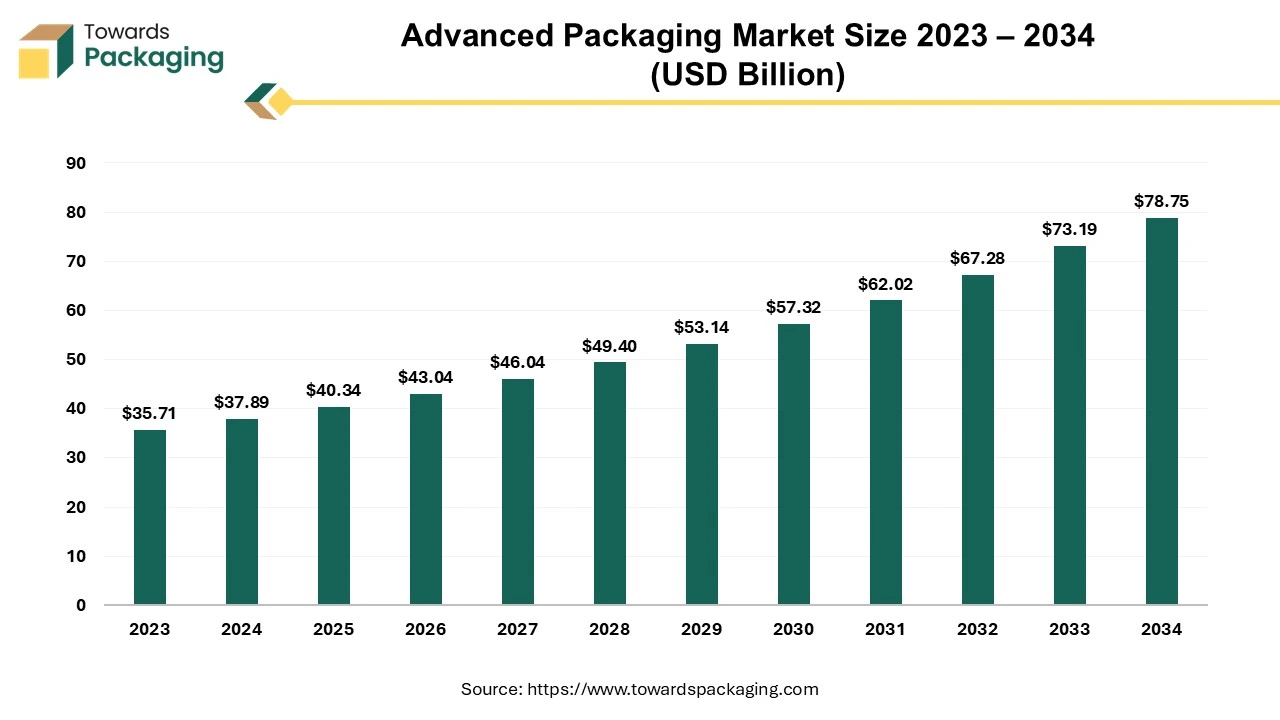
The advanced packaging market is expected to expand from USD 40.34 billion in 2025 to USD 78.75 billion by 2034, registering a CAGR of 7.59% throughout the forecast period. This growth is driven by increasing demand for high-performance, sustainable, and efficient packaging solutions across various industries.

The industry for advanced packaging is set to achieve substantial development in the years ahead. Multiple semiconductor chips are combined into a single chip package using a variety of manufacturing techniques known as advanced semiconductor packaging. This method lowers costs and power consumption while increasing capabilities. The most widely used methods in advanced packaging are system-in-package, fan-out wafer-level packaging, heterogeneous integration, 2.5D, and 3D-IC.
The integrated circuit packaging market is booming, poised for a revenue surge into the hundreds of millions from 2026 to 2035, driving a revolution in sustainable transportation.The growing demand for electronic products such as smartphones and other miniature electronics products has raised the demand for the market.
Integrated circuits are commonly known as microchips or chips. It is a set of electronic circuits that has several components and their interconnections. These small components are fabricated on a flat piece of semiconductor. It is primarily used for manufacturing electronic devices that are smaller in size. It is more reliable as this has a low risk of losing connection, like in other wiring. Many major market players are significantly evolving this market with advancements in wiring and helping companies to build compact yet effective devices. With the growing adoption of faster, smaller, and more efficient electronic devices, integrated circuit packaging technology, such as 3D packaging, flip-chip, and wafer-level packaging, is observed to spread rapidly. This market is majorly involved with the industry who are popular for manufacturing electronic products.
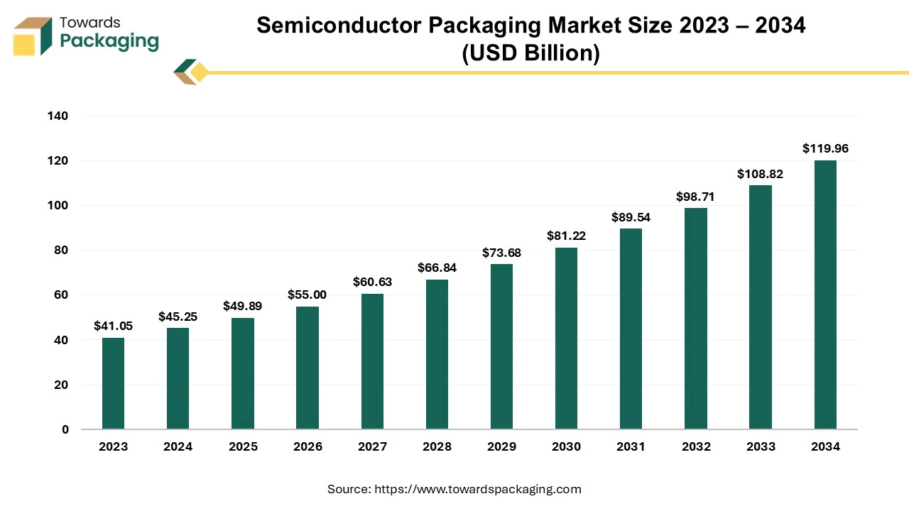
The semiconductor packaging market is expected to increase from USD 49.89 billion in 2025 to USD 119.96 billion by 2034, growing at a CAGR of 10.24% throughout the forecast period from 2026 to 2035.

A semiconductor is a material that can be used as the basis for computers and other electronic devices because of its unique electrical properties. Usually, it is a solid chemical element or compound that, in some situations, transmits electricity and, in others, does not. Due to this, it’s the perfect medium for managing electrical current in household equipment. The characteristics of semiconductor lie between those of an insulator and a conductor. Semiconductor are used to create transistors, integrated circuits (ICs), and diodes.
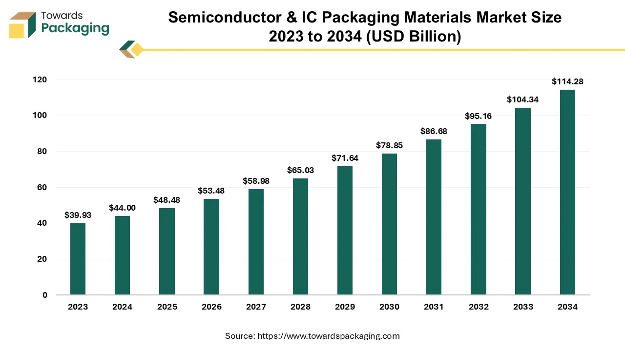
The semiconductor and IC packaging materials market is expected to grow from USD 48.48 billion in 2025 to USD 114.28 billion by 2034, with a CAGR of 10.2% throughout the forecast period from 2026 to 2035.

Constant innovations and development in packaging processes and materials s enhance yield and minimize costs, making advanced packaging solutions more attractive. The key players operating in the market are focused on adopting inorganic growth strategies like acquisition and merger to develop advance technology for manufacturing semiconductor & IC packaging materials which is estimated to drive the global semiconductor & IC packaging materials market over the forecast period.
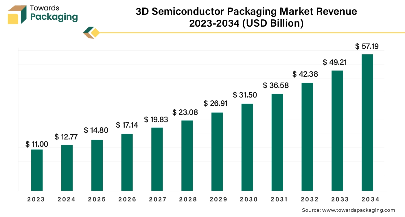
The global 3D semiconductor packaging market size was valued at US$ 11.00 billion in 2023 and is projected to hit US$ 57.19 billion by 2034, upsurging at a CAGR of 16.17% during the forecast period from 2026 to 2035. With widespread digitalization, 3D semiconductor industry is growing that is directly boosting the demand for 3D semiconductor packaging market.

Increased trend for miniaturization of electric devices has risen demand for the 3D packaging semiconductor. The key players operating in the market are focused on adopting inorganic growth strategies like acquisition and merger to develop advance technology for manufacturing 3D packaging for semiconductors which is estimated to drive the global 3D semiconductor packaging market over the forecast period. Increasing in adoption of the advanced technology for the production of 3D packaging semiconductor is estimated to drive the growth of the global 3D semiconductor packaging market in the near future.
By Packaging Technology
By Application
By End User
By Region

Research & Advisory Analyst
Yogesh Kulkarni is an experienced Research Analyst specializing in the packaging sector, with a strong foundation in statistical analysis and market intelligence. He currently contributes his expertise to Towards Packaging.
Learn more about Yogesh Kulkarni
Reviewed By
Aditi Shivarkar, with 14+ years in packaging market research, specializes in food, beverage, and eco-friendly packaging. She ensures accurate, actionable insights, driving Towards Packaging Analytics & Consulting 's excellence in industry trends and sustainability.
Learn more about Aditi Shivarkar3d IC and 2.5d IC Packaging Market