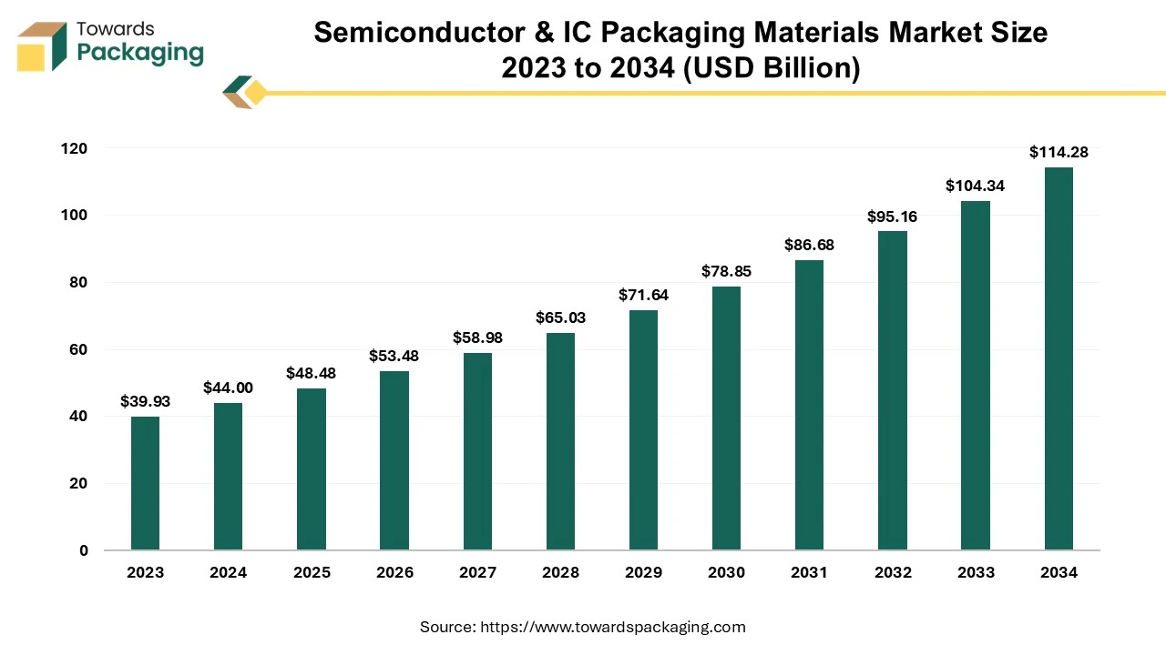
The semiconductor & IC packaging materials market is forecasted to expand from USD 53.43 billion in 2026 to USD 128.07 billion by 2035, growing at a CAGR of 10.2% from 2026 to 2035. This section covers the overall market size and growth drivers, and presents segmentation by product type, packaging technology and end‑use, offering a clear picture of how each segment contributes to the total.

Constant innovations and development in packaging processes and materials s enhance yield and minimize costs, making advanced packaging solutions more attractive. The key players operating in the market are focused on adopting inorganic growth strategies like acquisition and merger to develop advance technology for manufacturing semiconductor & IC packaging materials which is estimated to drive the global semiconductor & IC packaging materials market over the forecast period.
Semiconductor packaging refers to the process of enclosing semiconductor devices (like integrated circuits, or ICs) to protect them and connect them to other electronic components. This packaging is crucial for ensuring the functionality, reliability, and performance of electronic devices. Semiconductor & IC packaging protects delicate semiconductor materials s from environmental factors such as moisture, dust, and physical damage. It provides the necessary connections to other circuit elements.
The packaging facilitates the integration of ICs into electronic systems through pins or pads. Semiconductor and ICs generate heat during operation, and packaging plays a vital role in dissipating this heat to maintain performance and prevent failure. Semiconductor & IC packaging adds structural integrity, helping to withstand mechanical stresses during manufacturing and use. The packaging industry size is growing at a 3.16% CAGR.
The design and size of the package affect the overall form factor of the device, impacting the design and layout of electronic circuits. Components with leads that are inserted through holes in a printed circuit board (PCB). Common types include Dual In-line Package (DIP). Packages designed to be mounted directly onto the surface of a PCB, allowing for higher density and smaller sizes.
Various materials s utilized for semiconductor and IC packaging have been mentioned here as follows: silicon, epoxy resins, lead frames, ceramics, and organic substrates. As devices become smaller, packaging technologies evolve to allow for more compact designs, such as 3D stacking and advanced interconnects. New materials s and designs are being developed to improve heat dissipation, which is critical for high-performance applications. Combining various functions (e.g., RF, analog, digital) into a single package to improve efficiency and reduce costs.
Semiconductor and IC packaging is a vital aspect of electronics manufacturing, influencing device performance, reliability, and integration. As technology advances, the packaging landscape will continue to evolve, adapting to the demands of new applications and innovations in the electronics industry.
AI algorithms can analyze and simulate various design parameters to optimize packaging for thermal performance, size, and reliability. This can lead to innovative materials and configurations that improve efficiency. Machine learning models can detect defects in packaging materials during production by analyzing visual data, ensuring higher quality and reducing waste. AI can monitor equipment in real-time, predicting when maintenance is needed, which reduces downtime and prolongs the life of manufacturing tools.
AI can optimize supply chain logistics by predicting demand, managing inventory levels, and improving procurement strategies, leading to cost reductions and better resource allocation. AI can assist in the discovery of new materials by predicting properties and behaviours of combinations that have not yet been tested, fostering innovation in packaging solutions. AI-driven automation can streamline manufacturing processes, reducing human error and increasing production speed, which is crucial for meeting market demands.
Advanced analytics can provide insights into production processes, helping to identify trends and areas for improvement, ultimately leading to better decision-making. AI can help develop eco-friendly packaging materials by optimizing formulations and reducing waste throughout the production process. Overall, integrating AI in this sector can lead to enhanced efficiency, improved product quality, and innovative solutions, driving the industry forward.
The automotive industry's shift towards electric vehicles (EVs) and advanced driver-assistance systems (ADAS) increases the demand for reliable semiconductor packaging. Electric vehicles incorporate numerous electronic components, including power management systems, battery management systems, and advanced infotainment systems, all requiring efficient packaging solutions. Developments in battery technology, such as solid-state batteries, require specialized semiconductor packaging to ensure performance and safety.
Stricter emissions regulations drive the adoption of electric vehicles, further boosting the need for efficient and reliable electronic systems in these vehicles. The overall growth of the electric vehicles market accelerates demand for semiconductor components, thereby increasing the need for packaging materials that support these innovations. These factors collectively contribute to the rising demand for semiconductor and IC packaging materials in the electric vehicles sector.

The key players operating in the semiconductor & IC packaging materials market are facing difficulty in procuring raw materials and in meeting strict rules set by the government. The costs associated with advanced packaging technologies can be prohibitive, limiting investment in new materials and processes. The increasing complexity of semiconductor devices requires sophisticated packaging solutions, which can complicate development and manufacturing processes. Emerging technologies such as advanced 3D packaging and chiplet architectures may outpace traditional packaging methods, impacting market growth.
Global supply chain issues, exacerbated by events like the COVID-19 pandemic, can affect the availability and pricing of raw materials. Stricter environmental regulations regarding materials and manufacturing processes can increase compliance costs and limit certain practices. Fluctuations in demand for electronics can lead to uncertainty in the semiconductor market, affecting investments in packaging technologies. These factors collectively influence the market dynamics and can hinder growth potential.
With the increasing use of tablets, smartphones, and consumer electronics, there is a heightened demand for advanced and next-generation semiconductor packaging. The proliferation of IoT devices is driving the need for smaller, more efficient packaging solutions. The key players operating in the market are focused on innovating and launching new electronic devices which require compact semiconductor and IC packaging materials, which has created lucrative opportunity for the growth of the semiconductor & IC packaging materials market in the near future.
For instance,
| Rank | Company | Headquarters | Country | Why Relevant to This Market | Key Products/Services |
| 1 | Resonac Holdings | Tokyo | Japan | Global leader in semiconductor packaging materials | Epoxy molding compounds, die attach, underfills |
| 2 | Henkel | Düsseldorf | Germany | Leading supplier of advanced semiconductor adhesives | Die attach, underfills, thermal materials |
| 3 | Namics Corporation | Niigata | Japan | Major supplier of advanced IC packaging materials | Underfills, encapsulants, conductive adhesives |
| 4 | Ajinomoto | Tokyo | Japan | Pioneer of ABF substrate materials | Ajinomoto Build-up Film (ABF) |
| 5 | Shin-Etsu Chemical | Tokyo | Japan | Global supplier of semiconductor packaging materials | Encapsulation materials, silicones, photoresists |
| Rank | Company | Headquarters | Country | Why Relevant to This Market | Key Products/Services |
| 1 | Indium Corporation | Clinton, New York | USA | Leading solder material supplier | Solder pastes, solder balls |
| 2 | Mitsubishi Gas Chemical | Tokyo | Japan | Strong supplier of BT resin materials | BT substrates, specialty chemicals |
| 3 | Mitsui Mining & Smelting | Tokyo | Japan | Important supplier of semiconductor metals | Lead frames, copper materials |
| 4 | JX Advanced Metals | Tokyo | Japan | Advanced copper and sputtering materials | Electronic materials, copper products |
| 5 | Sumitomo Bakelite | Tokyo | Japan | Established supplier of molding compounds | Epoxy molding compounds |
| Rank | Company | Headquarters | Country | Why Relevant to This Market | Key Products/Services |
| 1 | MacDermid Alpha Electronics Solutions | Waterbury, Connecticut | USA | Specialty semiconductor packaging materials | Solder materials, adhesives |
| 2 | Nagase & Co. | Tokyo | Japan | Specialty electronic materials distribution | Functional packaging materials |
| 3 | Hitachi Chemical Advanced Materials | Tokyo | Japan | Advanced packaging material portfolio integrated into Resonac | Specialty packaging materials |
| 4 | Dexerials | Tochigi | Japan | High-performance electronic materials | Adhesives, conductive films |
| 5 | AI Technology | Princeton Junction, New Jersey | USA | Niche semiconductor packaging materials | Die attach adhesives, encapsulants |
SEMI formally initiated Workforce Development Program in India with a recent workshop on Semiconductor Manufacturing, hosted in conjunction with ESSCI at IT Delhi. This was part of SEMI's continuous efforts to drive the growth of semiconductors in India. The program places a strong emphasis on working in tandem with academic institutions to jointly develop skill development initiatives and specialized curriculum for semiconductor design roles. In an effort to close the talent gap in the semiconductor industry worldwide, India's strong engineering pipeline will now have the skills needed to prepare graduates for employment in the rapidly expanding field.
SEMICON India offers more SEMI initiatives to promote industry expansion, like Smart Manufacturing and Sustainability, supporting the Government of India's and the ISM's supportive regulatory policies and easing international investment to bolster India's standing in the sector. In addition to showcasing their vision and policies intended to draw major investments and spur growth, representatives from Tamil Nadu, Gujarat, Assam, Karnataka, Odisha, and Uttar Pradesh will also highlight India's shared goal of becoming a major participant in the world semiconductor scene.
The organic substrate segment held a dominant presence in the semiconductor & IC packaging materials market in 2025. Organic substrates offer excellent thermal stability, electrical performance, and reliability, making them suitable for advanced applications. They are generally more affordable compared to traditional materials like ceramics, facilitating wider adoption in various applications. Organic substrates are lighter than traditional materials, contributing to the overall reduction in weight for electronic devices, which is essential for portable technologies. The organic semiconductors have ability to manage heat effectively.
Organic substrate is compatible with smaller, denser designs supports the industry trend toward miniaturization and increased functionality in compact formats. Increasing focus on eco-friendly materials makes organic substrates appealing due to their potential for lower environmental impact compared to traditional materials. The key players operating in the are focused on developing and launching semiconductor & IC packaging and packaging materials utilizing organic substrate which is estimated to drive the growth of the segment over the forecast period.
For instance,
The small outline package (SOP) segment accounted for a significant share of the semiconductor & IC packaging materials market in 2025. Small Outline Package (SOPs) are designed to occupy less board space, making them ideal for compact electronic devices, which is crucial in consumer electronics and mobile applications.
Small Outline Packaging (SOPs) are easier to handle during assembly processes, contributing to faster production times and reduced labor costs. They generally have lower manufacturing costs compared to other packaging types, making them attractive for mass production.
Small Outline Packaging (SOPs) often provide adequate thermal management, essential for reliable operation in high-performance applications. They can be used for a wide range of applications, including analog, digital, and mixed-signal devices, broadening their market appeal.
The robust construction of Small Outline Packaging (SOPs) enhances reliability, which is crucial in automotive, industrial, and telecommunications applications. Small Outline Packaging (SOPs) are well-suited for automated assembly lines, supporting the industry's shift towards automation and efficiency. These factors collectively contribute to the dominance of the Small Outline Package segment in the semiconductor and IC packaging materials market.
The consumer electronics segment registered its dominance over the global semiconductor & IC packaging materials market in 2025. The demand for smaller, more compact devices drives the need for advanced packaging solutions that save space without compromising performance. IC packaging materials can be adapted for a wide range of applications, from smartphones to home appliances, making them suitable for diverse consumer electronics. High-performance packaging materials ensure efficient heat dissipation and electrical connectivity, crucial for the functioning of modern electronics.
As consumer electronics evolve, incorporating features like AI, 5G, and IoT, advanced semiconductor packaging is essential to support these technologies. The fast-paced nature of consumer electronics requires packaging solutions that can keep up with frequent product updates and new technology integrations. These factors make semiconductors and IC packaging materials integral to the success and advancement of consumer electronics. Moreover, the key players operating in the market are focused on developing advanced technology consumer electronics which has risen the demand of the semiconductor & IC packaging materials in the market.
For instance,
The 4K upscaling feature of the 2024 Crystal 4K TV series allows for the lifelike 4K picture quality by improving and upscales lower resolution content to match the higher resolution of a 4K display. With the splendor of HDR10+, PurColor, Crystal Processor 4, and One Billion True Colors, users can now experience superior contrast with deep blacks and dazzling lights.
Asia Pacific region held the dominating share of the semiconductor & IC packaging materials market in 2025. Countries like China, Japan, and South Korea have advanced manufacturing infrastructures, allowing for mass production of electronics at competitive prices. A rapidly growing middle class and increasing disposable income in countries like India and Southeast Asia boost demand for consumer electronics. Major tech companies in the region invest heavily in research and development, driving innovation in consumer electronics. The presence of a well-developed supply chain and logistics network facilitates quick turnaround times and cost efficiency.
The key players operating in the Asia Pacific market are focused on developing advanced semiconductor packaging technology, which is estimated to drive the semiconductor & IC packaging materials market in Asia Pacific region over the forecast period.
For instance,
China semiconductor & IC packaging materials market is growing owing to expansion of the domestic manufacturing capabilities in the country. China's "Made in China 2025" initiative aims to transform the country into a global leader in high-tech industries, with semiconductors being a central focus. To support this, the government has established the China Integrated Circuit Industry Investment Fund (also known as the "Big Fund"), which has invested heavily in domestic semiconductor companies. The third phase of this fund, launched in 2025, allocated approximately US$47.5 billion to bolster the semiconductor industry, emphasizing areas like advanced manufacturing and materials. Chinese companies have significantly increased their semiconductor manufacturing capacities.
For instance, Semiconductor Manufacturing International Corporation (SMIC) reported a 28% revenue increase in the first quarter of 2025, driven by strong demand and government support.
Additionally, domestic production of wafer fabrication tools rose to 11.3% of China's purchases in 2025, up from 5.1% in 2020, indicating a push towards self-sufficiency in manufacturing equipment. To meet the demands of emerging applications like AI and 5G, China is investing in advanced packaging solutions such as 3D packaging and System-in-Package (SiP) technologies. These innovations enable higher performance and integration in smaller form factors, essential for modern electronic devices.
China has established high-tech zones, such as the Zhangjiang Hi-Tech Park in Shanghai, to foster innovation and collaboration among semiconductor companies, research institutions, and universities. These ecosystems provide infrastructure and support for R&D, facilitating the growth of the semiconductor industry. Recognizing the importance of skilled professionals, China is enhancing education and training programs in semiconductor-related fields. Institutions like Tsinghua University's School of Integrated Circuits are cultivating domestic talent to support the industry's growth.
North America region is anticipated to grow at the fastest rate in the semiconductor & IC packaging materials market during the forecast period. The United States has the biggest market share in the North American semiconductor industry and has seen the fastest growth throughout the projected period due to its significant R&D investments, cutting-edge technological infrastructure, and robust ecosystem of semiconductor businesses. Big American semiconductor businesses like Texas Instruments, Qualcomm, and Intel are the ones driving continuous innovation in packaging technology.
The CHIPS Act, enacted by the US government, is a significant driver of the market's expansion as it provides significant funding for domestic semiconductor manufacture and packaging. By supporting domestic semiconductor manufacturing, this act seeks to lessen dependency on foreign semiconductor suppliers. The key players operating in the North America region are focused on carrying out research and development and funding for innovating semiconductor packaging technology, which is estimated to drive the semiconductor & IC packaging materials market in North America over the forecast period.
For instance,
U.S. semiconductor & IC packaging materials market is driven by the strategic government initiatives and technology advancements in the country. The CHIPS and Science Act, enacted in August 2022, allocates approximately US$52.7 billion to bolster domestic semiconductor manufacturing, research, and workforce development. This includes US$39 billion in manufacturing subsidies and US$13 billion dedicated to research and development, aiming to reduce dependency on foreign semiconductor suppliers and enhance national security. Major semiconductor companies have announced substantial investments to expand U.S. manufacturing capabilities.
For instance, Intel plans to invest nearly US$90 billion in U.S. facilities by the end of the decade, with significant projects in Arizona, New Mexico, Ohio, and Oregon. Similarly, Texas Instruments is set to receive up to US$1.6 billion under the CHIPS Act to aid the construction of new facilities in Texas and Utah, contributing to a total investment of US$18 billion through 2029.
The U.S. leads in developing advanced semiconductor packaging technologies essential for applications in AI, 5G, and high-performance computing. The National Advanced Packaging Manufacturing Program received US$3 billion in funding in November 2023 to accelerate innovation in this sector. Additionally, companies like Amkor Technology have announced plans to establish new facilities in the U.S., further enhancing domestic packaging capabilities.
The U.S. hosts a comprehensive semiconductor ecosystem, including leading companies such as Intel, AMD, and Texas Instruments, as well as research institutions and technology hubs like Silicon Valley. This ecosystem fosters innovation and supports the development of cutting-edge semiconductor technologies. The increasing demand for electronic devices, including smartphones, tablets, and IoT gadgets, drives the need for efficient and reliable semiconductor packaging materials. North America's focus on technological advancements and infrastructure development reinforces its dominant position in the global market.
By Product Type
By Packaging Technology
By End-Use
By Region

Research & Advisory Analyst
Yogesh Kulkarni is an experienced Research Analyst specializing in the packaging sector, with a strong foundation in statistical analysis and market intelligence. He currently contributes his expertise to Towards Packaging.
Learn more about Yogesh Kulkarni
Reviewed By
Aditi Shivarkar, with 14+ years in packaging market research, specializes in food, beverage, and eco-friendly packaging. She ensures accurate, actionable insights, driving Towards Packaging Analytics & Consulting 's excellence in industry trends and sustainability.
Learn more about Aditi ShivarkarSemiconductor and IC Packaging Materials Market